1 Introduction
In the circuit board assembly, solder paste is printed on the pads of the circuit board first, then various electronic components are mounted, and finally passed through a reflow furnace. After the solder balls in the solder paste are melted, the various electronic components and the circuit board are soldered. The plates are welded together to realize the assembly of the electronic module. This surface mount technology (SMT) is increasingly used in high-density packaging products, such as system in package (SiP) often soldered ball griarray (referred to as ball griarray). BGA) devices, power bare chips, quad flat no-lead (QFN) devices. Due to the characteristics of the solder paste soldering process and materials, after reflow soldering of these large soldering surface devices, voids will appear in the soldering area[1]. The voids will affect the electrical, thermal and mechanical properties of the product, and even lead to product failure[1] 2-4] Therefore, improving and solving solder paste reflow soldering voids has become a process technology problem that must be resolved. Some researchers have analyzed and studied the causes of BGA solder ball soldering voids, and provided improved solutions [5- 6], the conventional solder paste reflow soldering process has a QFN with a soldering area larger than 10 mm2 or a bare chip solution with a soldering area larger than 6 mm2.
Preform soldering and vacuum reflow furnace soldering are used to improve soldering voids. Prefabricated soldering pads need special equipment to apply flux. For example, directly mount the chip on the prefabricated soldering pad. After reflow, the chip is shifted and tilted seriously; if the chip is reflowed first, then the flux is applied to mount the chip. Two reflows increase the process. Prefabricated soldering And the cost of flux materials is much higher than that of solder paste. Vacuum reflow equipment is more expensive, the vacuum capacity of the independent vacuum chamber is very low, and the cost performance is not high. In addition, the problem of tin splashing is serious, and the application of high-density, small-pitch products is an important factor that restricts its application. This article is based on the conventional solder paste reflow soldering process and develops and introduces a new secondary reflow process to improve soldering voids and solve the problems of bonding and plastic packaging cracks caused by soldering voids.
2. Solder paste printing reflow soldering voids and their generation mechanism
2.1 Welding void
After reflow soldering, the product is inspected under X-ray. The lighter color of the soldering area is the void due to insufficient solder in the soldering layer, as shown in Figure 1.
2.2 Welding void generation mechanism
Take SAC305 solder paste as an example. The main composition and functions are shown in Table 1. The flux and tin beads are glued together in a paste form. The weight ratio of tin solder to flux is about 9:1, and the volume ratio is about 1:1. .
Element
|
Element
|
weight ratio/%
|
function
|
|
tin
|
85~92
|
Welding, connecting various electronic components and circuit boards
|
|
soldering flux
|
2~8
|
Increases viscosity and removes metal oxides
|
|
adhesion agent
|
1~2
|
Prevent oxidation of solder surface
|
|
active agent
|
0~1
|
Removal of metal oxides
|
|
solvent
|
1~7
|
Stickiness and printing adjustment
|
Table 1 The main composition and function of solder paste
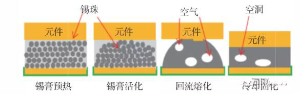
After the solder paste is printed and mounted with various electronic components, when it passes through the reflow oven, the solder paste will go through four stages: preheating, activation, reflow, and cooling. The temperature in different stages is different, and the state of the solder paste is also different. as shown in picture 2.
Figure 2 Schematic diagram of solder paste temperature curve at different stages of reflow soldering
In the preheating and activation stages, the volatile components in the solder paste in the solder paste will volatilize into gas when heated. At the same time, gas will also be generated when the surface oxide of the solder layer is removed. Part of these gas will volatilize and separate from the solder paste. The solder balls are caused by flux. Volatile and compactly gather; in the reflow stage, the remaining flux in the solder paste will quickly volatilize, the tin beads will melt, a small amount of flux volatile gas and most of the air between the tin beads are not dispersed in time, and remain in the molten tin Under the tension of molten tin, it forms a hamburger sandwich structure and is clamped by circuit board pads and electronic components. The gas wrapped in liquid tin can hardly escape only by buoyancy, and the molten state time is very short. When the molten tin cools down and becomes solid tin, pores appear in the solder layer [7], and solder voids are generated, as shown in Figure 3.
Image
Figure 3 Schematic diagram of the generation principle of solder paste reflow soldering voids
The root cause of solder voids is that the air or volatile gas contained in the solder paste is not completely discharged after the solder paste is melted. The influencing factors include solder paste material, solder paste printing shape, solder paste printing volume, reflow temperature, reflow time, solder size, structure Wait.
advertise
3. Verification of influencing factors of solder paste printing reflow soldering voids
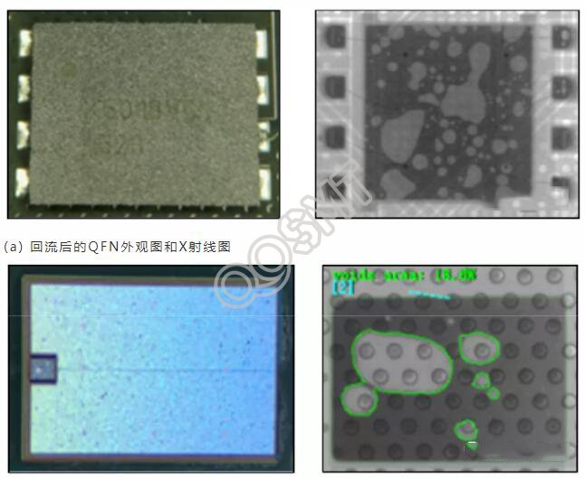
Use QFN and bare chips to test and confirm the main causes of reflow soldering voids, and find ways to improve solder paste printing reflow soldering voids. The cross-section of QFN and bare chip solder paste reflow soldering products is shown in Figure 4. The QFN soldering surface size is 4.4 mm×4.1 mm, and the soldering surface is tin-plated (100% pure tin); the bare chip soldering size is 3.0 mm×2.3 mm , The soldering layer is a sputtered nickel-vanadium bimetallic layer, and the surface layer is vanadium; the substrate pads are electroless nickel-palladium immersion gold with thicknesses of 0.4 μm /0.06 μm/0.04 μm; SAC305 solder paste is used, and the solder paste printing equipment is DEK Horizon APiX, the reflow oven equipment is BTU Pyramax 150N, and the X-ray inspection equipment is DAGE XD7500VR.
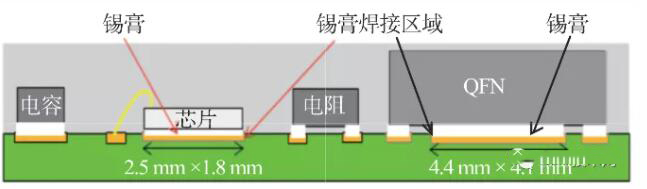
Fig. 4 is a cross-sectional view of QFN and bare chip solder paste reflow soldering products. In order to facilitate the comparison of test results, reflow soldering is performed under the conditions in Table 2.
After surface mounting and reflow soldering were completed, the soldering layer was inspected by X-ray, and it was found that the soldering layer at the bottom of the QFN and bare chip had large cavities, as shown in Figure 5.
(a) Appearance and X-ray diagram of QFN after reflow
(b) The appearance and X-ray diagram of the chip after reflow
Since the size of the tin ball, the thickness of the stencil, the opening area rate, the shape of the stencil, the reflow time, and the peak furnace temperature will affect the reflow soldering voids, there are many influencing factors, which can be directly verified by the DOE test. Quickly screen and determine the main influencing factors through the correlation comparison test, and then further optimize the main influencing factors through DOE.
3.1 Soldering void and solder paste solder ball size
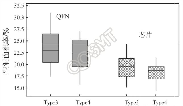
Tested with type3 type (tin bead size of 25~45μm) SAC305 solder paste, other conditions remain unchanged, after reflow, the solder layer voids are measured and compared with type4 solder paste. It is found that the solder layer voids of the two solder pastes are not significantly different, indicating that they are different The solder paste with the size of the tin beads has no obvious effect on the voids of the soldering layer, and is not an influencing factor, as shown in Figure 6.
Figure 6 Comparison of solder layer voids of solder paste with different solder ball sizes
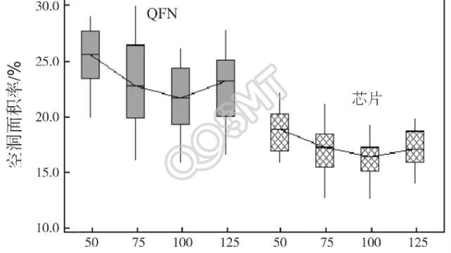
3.2 Welding void and printing stencil thickness
Tests with 50μmm, 100μm, 125μm thickness printed stencils, other conditions remain unchanged, after reflow, the void area of the solder layer is measured and compared with the 75μm thickness printed stencil. It is found that different stencil thicknesses (the amount of solder paste) affect the QFN and chip Welding layer voids have a certain effect. As the thickness of the steel mesh increases, the void area gradually decreases. When it reaches a certain thickness (100μm), the void area will reverse and increase as the thickness of the steel mesh increases, as shown in Figure 7. This means that the amount of solder paste increases and the reflowed liquid tin is covered by the chip, and the outlets for residual air to escape are only narrow. When the amount of solder paste is changed, the outlets for residual air to escape also increase. The instant burst of the volatile gas escaping the liquid tin will cause the liquid tin to splash around the QFN and the chip. The test found that the increase of the thickness of the steel mesh will increase the burst of air or volatilized air bubbles, and the probability of tin splashing and contamination around the QFN and chips will increase accordingly.
Image
Figure 7 Comparison of welding layer voids under different thickness steel mesh conditions
3.3 Welding cavity and steel mesh opening area ratio
Tests with printed stencils with opening ratios of 100%, 90%, and 80%. Other conditions remain unchanged. After reflow, the void area of the solder layer is measured and compared with the printed stencil with 100% opening ratio. It is found that the opening ratios are 100%, 90%. Under the conditions of% and 80%, there is no obvious difference between the welding layer voids, as shown in Figure 8.
Figure 8 Comparison of welded layer voids under different stencil opening ratios
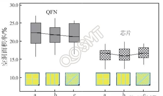
3.4 Welding cavity and printed stencil shape
Use strip type b, diagonal grid type c solder paste printing shape test, other conditions remain unchanged, after reflow, measure the void area of the soldering layer and compare it with the grid type a printing shape, find grid type, long strip type, diagonal grid There is no obvious difference in the welding layer voids under the type conditions, as shown in Figure 9.
Figure 9 Comparison of voids in the welded layer under different stencil shapes
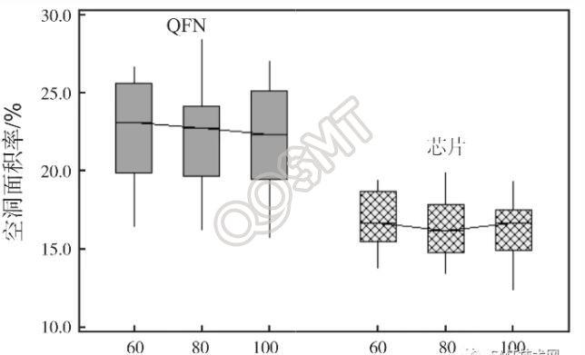
3.5 Soldering void and reflow time
Extend the reflow time (70 s, 80 s, 90 s) test, other conditions remain unchanged, measure the solder layer voids after reflow, and compare with the 60 s reflow time, it is found that the reflow time increases, the solder void area decreases, but the magnitude is reduced It gradually decreases with time, as shown in Figure 10. This shows that when the reflow time is insufficient, increasing the reflow time is beneficial to the full overflow of the air wrapped in the molten liquid tin, but after the reflow time increases to a certain period of time, the air wrapped in the liquid tin is difficult to overflow. Reflow time is a factor that affects solder voids.
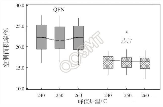
3.6 Welding void and peak furnace temperature
Use 240 ℃, 250 ℃ peak furnace temperature test, other conditions remain unchanged, measure the void area of the solder layer after reflow, and compare with the peak furnace temperature of 260 ℃, it is found that the solder layer of QFN and chip is void under different peak furnace temperature conditions There is no obvious change, as shown in Figure 11. It shows that different peak furnace temperatures have little effect on the voids in the soldering layer of QFN and chips, and it is not an influencing factor.
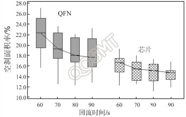
Figure 10 Comparison of solder layer voids under different reflow times
Figure 11 Comparison of welding layer voids under different peak furnace temperatures
The above test shows that the significant factors affecting the voids of the soldering layer of QFN and chips are reflow time and stencil thickness.
4. Improvement of solder paste printing reflow soldering voids
4.1 DOE test to improve welding voids
Improve QFN and chip soldering layer voids by finding the optimal value of the main influencing factors (reflow time, stencil thickness). The solder paste is SAC305 type4, the stencil shape is grid type (100% opening degree), and the peak furnace temperature It is 260 ℃, and other test conditions are the same as the test equipment. The DOE test and results are shown in Table 3.
|
serial number |
Screen Stencil Thickness/um
|
refluxing time/s
|
QFNcavity
|
chip Cavity
|
|
1
|
50
|
60
|
27.80%
|
20.50%
|
|
2
|
50
|
70
|
23.30%
|
17.90%
|
|
3
|
50
|
80
|
22.80%
|
17.60%
|
|
4
|
50
|
90
|
24.50%
|
19.30%
|
|
5
|
75
|
60
|
24.60%
|
19.40%
|
|
6
|
75
|
70
|
23.10%
|
18.40%
|
|
7
|
75
|
80
|
19.10%
|
16.50%
|
|
8
|
75
|
90
|
19.80%
|
18.40%
|
|
9
|
100
|
60
|
21.70%
|
17.60%
|
|
10
|
100
|
70
|
17.60%
|
14.70%
|
|
11
|
100
|
80
|
16.10%
|
14.50%
|
|
12
|
100
|
90
|
18.60%
|
16.40%
|
|
13
|
125
|
60
|
24.40%
|
17.20%
|
|
14
|
125
|
70
|
20.10%
|
16.60%
|
|
15
|
125
|
80
|
20.80%
|
15.40%
|
|
16
|
125
|
90
|
20.70%
|
18.10%
|
Table 3 "Welding void DOE and test results
The influence of stencil thickness and reflow time on QFN and chip soldering voids is shown in Figure 12. Through the interaction analysis of the main influencing factors, it is found that using 100μm stencil thickness and 80 s reflow time can significantly reduce the soldering voids of QFN and chip. The soldering void rate of QFN is reduced from the maximum of 27.8% to 16.1%, and the chip soldering void rate is reduced from the maximum of 20.5% to 14.5%. In the experiment, 1000 products were produced under the optimal conditions (100μm stencil thickness, 80 s reflow time), and the soldering void rate of 100 QFNs and chips were randomly measured. The average soldering void rate of QFN was 16.4%, and the soldering void of the chip The average rate is 14.7%. Compared with the improvement before, the solder void rate of QFN and chip has been significantly reduced.
4.2 The new process improves welding voids
Actual production conditions and experiments show that when the soldering cavity area at the bottom of the chip is less than 10%, there will be no chip cavity position cracking during wire bonding and molding. Through the DOE optimized process, please refer to Yang Jianwei: Conventional solder paste The analysis and resolution of reflow soldering voids cannot meet the requirements of soldering voids, and it is necessary to further reduce the soldering void area rate of the chip.
Since the chip covered on the solder prevents the gas in the solder from floating and escaping, in order to further reduce the void rate at the bottom of the chip, it is achieved by eliminating or reducing the solder wrapping gas. Adopting two new solder paste printing and reflow soldering processes: one solder paste printing, one reflow does not cover the QFN and bare chip to exhaust the gas in the solder; the second solder paste printing, mounting, and second reflow, the specific process is shown in
For the first printing of 75μm thick solder paste, most of the gas in the solder that is not covered by the chip floats and escapes through reflow, and the thickness after reflow is about 50μm; after one reflow is completed, small squares are printed on the surface of the cooled and solidified solder. (In order to reduce the amount of solder paste, reduce the amount of gas overflow, reduce or eliminate solder spatter), 50μm thick solder paste (the foregoing test results show that 100 μm is the best, so the secondary printing thickness is 100μm-50μm=50μm), and then mount the chip, and then reflow through 80 s. The solder after the first printing and reflow has almost no voids, and the amount of solder paste in the secondary printing is very small, and the soldering voids are small.
4.3 Welding cavity effect verification
Produce 2000 products (the thickness of the stencil for the first printing is 75μm, and the thickness of the stencil for the second printing is 50μm), other conditions are unchanged, the soldering void rate of 500 QFNs and chips are randomly measured, and it is found that there is no void after the first reflow of the new process. After the second reflow, the maximum solder void rate of QFN is 4.8%, and the maximum solder void rate of chips is 4.1%. Compared with the original solder paste printing and soldering process and the optimized DOE process, solder voids are significantly reduced. , As shown in Figure 15. After the functional tests of all products, no chip cracks were found.
5. Summary
Although optimizing solder paste printing volume and reflow time can reduce the solder void area, the solder void rate is still large. The use of two solder paste printing reflow soldering processes can effectively and maximize the solder void rate, and mass production can realize QFN circuits The soldering void ratio of the bare chip soldering area of 4.4 mm×4.1 mm and 3.0 mm×2.3mm is controlled below 5%, which improves the quality and reliability of reflow soldering. The research in this paper provides an important reference for improving the welding void problem of larger area welding surface.