How to solve the tombstone defect of 0201 and 01005 components? --Start with defect mechanism, root cause, and improvement measures
Oct 19, 2021
1. Frontier
The development trend of electronic products is more and more functions, lighter weight, lower prices, and higher density. The requirements for components are more and more miniaturized, which is not only manifested in such as BGA, The size of active devices in CSP, QFP and other package forms has been reduced, the pin spacing has become smaller, and the size of discrete components such as capacitors and resistors has also decreased accordingly. Figure 1 shows the development trend of electronic products and the impact on devices and PCBs. New challenges coming.
Due to the multi-functional and high-density development trend of mobile terminal products such as smart phones, the mounting density of components inside the mobile phone is increasing rapidly, and the use of micro chip components is increasing.
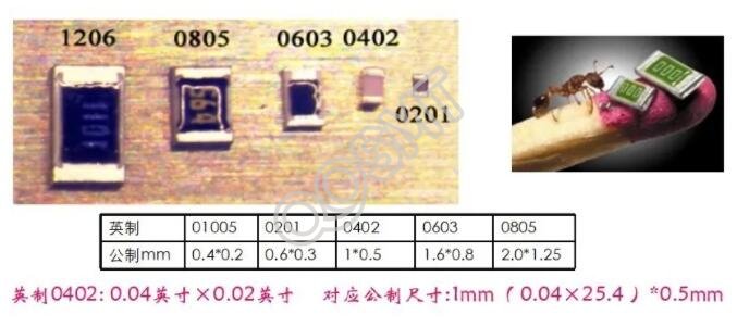
With the rapid increase in the use of these 0402 (1mm*0.5mm), 0201 (0.6mm*0.3mm), and even 01005 (0.4mm*0.2mm) micro-packaged components, and the continuous improvement of layout density, the difficulty of assembly continues to increase. The processing defects faced by the assembly of micro-chip components have become the main challenge in electronic assembly, and one of the most common defects of micro-chip components is tombstone.
The trend of component miniaturization and the comparison of the size of 0402, 0201 resistors, firewood heads and ants
2. Mechanism analysis of tombstone process defects
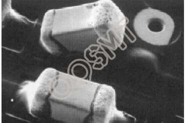
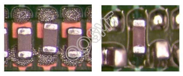
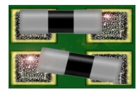
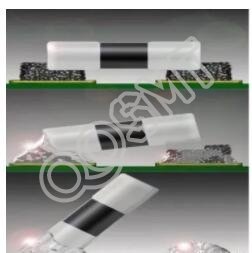
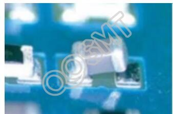
Tombstones are called "tombstoning, drawbridging, stonehenging and Manhattan" phenomena in the electronics manufacturing industry, and they are all used to describe the chip component welding process defects as shown in Figure 3. The vivid statement of this type of defect is that one end of the component is tilted to a certain angle during the reflow soldering process.
In the early SMT soldering process, the tombstone phenomenon is a process defect that is strongly related to vapor reflow soldering and infrared reflow soldering. In gas phase reflow soldering, the main reason for tombstone formation is that the component heats up too fast, and there is no soaking process to melt the solder paste when the temperature rises. As a result, the solder paste at both ends of the component with different heat capacity is not melted at the same time, so the two devices The imbalance of the wetting force at the end causes the tombstone phenomenon to occur.
For infrared reflow soldering, the difference in the color of the pad, solder paste, and solder tip will cause the difference in heat absorption, which will cause the solder paste at both ends to melt at the same time.
Tombstone defects in the soldering process of chip components
Later, with the improvement of the quality of chip component soldering ends, the widespread use of hot-air reflow soldering, and the optimization of reflow curves, the tombstone phenomenon gradually decreased, which is no longer an important issue in the SMT assembly process.
However, with the miniaturization of electronic components in recent years, especially the large-scale use of 0402, 0201, 01005 packaged devices in mobile terminal products, the tombstone defect has become a major defect in the SMT process. Costs have had a big impact.
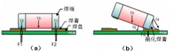
Analyzed from the mechanism, the essential cause of the tombstone defect is the imbalance of the wetting force at both ends of the device. When the rotating torque generated by the wetting force at one end exceeds the combined torque of the wetting force at the other end and the gravity of the device, the moment Under the action of, one end of the component is lifted up, and the force process of the component is shown in Figure 4.
Mechanical analysis of tombstone phenomenon
Figure 4a shows the stress state of the device after component placement and before reflow soldering. Figure 4b shows the stress state of the device during the tombstone reflow soldering. After placement and before reflow soldering, the device receives the adhesive force and supporting force F1 at both ends of the component. , F2 and gravity. When the tombstone of the welding process occurs, the device will flip under the combined action of the bonding force T2 at the pulling end, the gravity T3 of the device, and the wetting force T4 and T5 at the melting end. At this time, T4 produces the support point of the welding end. The moment of is greater than the sum of moments produced by T2+T3+T5 butt welding end support points, namely:
M(T4)>M(T2)+M(T3)+M(T5) (1)
It can be seen from Figure 4 that the smaller the components and the lighter the weight, the easier it is to tombstone.
The meaning of each parameter in Figure 4:
T1, T2 component welding end adhesion force
The supporting force received by the welding end of F1 and F2 components
M(T2) Moment generated by the bonding force T2 of the component welding end
Gravity of T3 element
M(T3) The moment produced by the gravity T3 of the element
Wetting force at the end of T4 element
M(T4) Moment generated by the wetting force T4 at the end of the element
T5 Wetting force at the bottom of the solder end of the component
M(T5) Moment generated by the wetting force T5 at the bottom of the solder end of the component
3. Factors affecting the tombstone of chip components
3.1 The influence of pad design on the formation of tombstone defects
The larger the pad size of the component, the larger the surface area of the molten solder, the greater the wetting force produced on the solder end, and the more significant the impact on the tombstone. The IPC standard has recommendations for the design of the pad size, but the size of the same type of device varies from manufacturer to manufacturer.
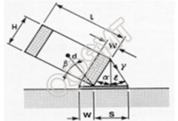
As shown in Figure 5, the two pad sizes that have the greatest impact on the tombstone phenomenon are W and S. When W is greater than S, the torque generated by the end wetting force is smaller than when W is less than S, and the probability of tombstoning is smaller. . Therefore, in the design stage, attention should be paid to the size of the pad, and the size of the integrated device can be designed with a reasonable pad, thereby effectively reducing the occurrence of tombstones.
The pad size that affects the tombstone
3.2 The influence of solder paste printing on the formation of tombstone defects
When the solder paste printing has deviations, the solder paste is not accurately printed on the pads. As shown in Figure 6, the solder paste printing on the upper pads is offset, and the device terminals are not in good contact with the solder paste after mounting. When reflow soldering in the furnace, the solder paste will not climb to the solder end of the component, and the two ends of the device have wetting power while the other end has no wetting power, and there will be a serious torque imbalance, and there will be no contact with the solder paste. One end was pulled up and a tombstone appeared.
Figure 6 shows a relatively serious printing failure, sometimes due to poor printing effects, resulting in a large difference in the amount of solder paste at both ends of the pad. At this time, the wetting force of the two ends will also have a large difference during reflow soldering. A certain degree of difference will lead to the occurrence of tombstones.
The offset of the solder paste printing leads to the tombstone of the component
3.3 The impact of placement accuracy on the formation of tombstone defects
If the placement accuracy of the placement machine is poor, the component end has a large offset relative to the pad during the placement process, and the contact area between the two ends of the component and the solder paste is different, and the wetting force at both ends of the component is unbalanced when the solder paste melts. Cause the tombstone to occur.
When it is more serious, the component placement deviation is large, and one end of the component is not in contact with the solder paste. During reflow soldering, the wetting force at both ends of the component is seriously unbalanced, resulting in tombstones. Therefore, for micro-chip components, the placement accuracy must be guaranteed, especially with the large-scale use of 0201, 01005 devices, the smaller the device, the more sensitive to various errors.
The influence of component placement deviation on tombstone defects
3.4 The influence of reflow temperature profile on the formation of tombstone defects
The reflow soldering temperature profile also has a greater impact on the production of tombstones. If the temperature profile is set improperly, such as the heating rate is too fast, the preheating time is too short, etc., this will cause a large temperature difference between the two ends of the device during reflow, which is serious. At this time, the solder paste on one end of the device has melted, but the other end has not yet melted. At this time, the imbalance of the wetting force at both ends will cause the device to tombstone.
Figure 8 shows a schematic diagram of the tombstone caused by the imbalance of the wetting force due to the large difference in the temperature of the solder paste at both ends, and the solder did not melt at the same time.
Unreasonable setting of reflow temperature curve leads to tombstone
3.5 The influence of material weldability on the formation of tombstone defects
The solderability of the solder ends of the device is inconsistent. For example, the solderability of one end is good, and the solderability of the other is poor. When reflow soldering, the wetting force of the melted solder to the soldering end with poor solderability will be less than that of the soldering end with good solderability. There will be a large force imbalance at both ends, leading to the occurrence of tombstones.
If one end of the PCB pad has poor solderability, and the other end has good solderability, when reflow soldering, for the poor solderability end, the molten solder will be sucked away by the soldering end of the device, so that the poor solderability end is soldered The wetting force of the disc to the device is very small, and the wetting force of the pad on the end with good solderability to the device will be greater, and at this time, a tombstone will still appear due to the imbalance of the wetting force. Figure 9 shows the tombstone defect caused by the difference in solderability of the solder ends of the chip components.
Tombstones caused by poor solderability of the solder ends of the device
4. Measures to solve the defects of the tombstone process
The tombstone defect is a preventable process defect, analyze its formation mechanism, summarize the root causes and influencing factors, and reduce the occurrence of tombstones through process design, quality control, process modulation, and equipment improvement, and improve the straight-through rate of the assembly process , Reduce the defect rate, reduce repairs, thereby improving the quality and reliability of electronic products.
When we have a full understanding of the mechanism of the tomb erection defect, we can sort out the main reasons for the tomb erection as shown in Figure 10:
Corresponding to the analysis of the mechanism and the main reasons, we can sort out the common measures to prevent the occurrence of tombstones:
1) Improve the level of DFM design, especially the design of the pad. The extension of the pad beyond the chip component terminal should be appropriate and not too large; the width of the pad should be appropriate, and the pad that exceeds the width of the device will be melted during reflow It will cause the device to drift, and the probability of tombstone will increase;
2) Ensure that the accuracy of the solder paste printing position is consistent with the amount of solder paste at both ends;
3) Ensure the accuracy requirements of the component placement position;
4) Reasonable setting of reflux curve: proper heating rate and preheating time to avoid excessive heating rate and short preheating time;
5) Ensure good solderability of the material: component solder ends, PCB pads and solder paste must have good solderability.
6) Error control: Including the size error of the solder end of the device and the size error of the PCB pad. The smaller the device, the more sensitive to the error.
...............
5. Summary
With the widespread use of microchip components such as 040, 0201, 01005 in electronic products, the analysis and resolution of tombstone defects have become a major problem that plagues SMT engineers.
This article starts from the analysis of the mechanism of the formation of the tombstone defects of the micro chip components, and through the analysis of various factors that affect the tombstone tombstone, various measures to solve the tombstone defects are proposed. This process defect has certain guiding significance.