SMT electronic manufacturing process technology analysis
Oct 20, 2021

Characteristics of SMT process technology


Recommended setting values for each section of the reflow temperature curve:
One of the following reasons can cause moisture to be entrained on the PCB
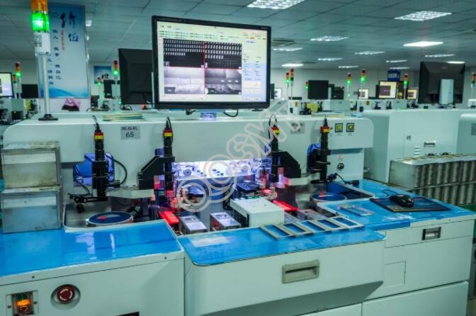
01 Practical SMT manufacturing and Summary of welding quality problem analysis
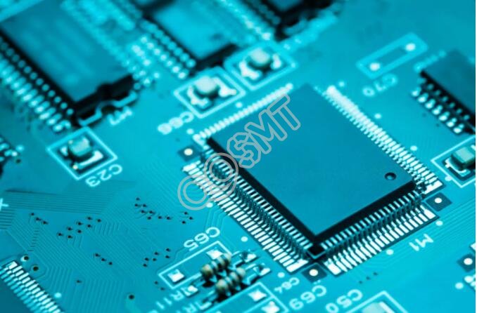
The Chinese name of PCB is printed circuit board, also known as printed circuit board, printed circuit board, circuit board, PCB circuit board, etc. It is an important electronic component, a support for electronic components, and a provider of electrical connections for electronic components. Because it is made by electronic printing, it is called a "printed" circuit board.
Characteristics of SMT process technology
The characteristics of SMT process technology can be compared with the traditional through-hole insertion technology (THT). From the perspective of assembly process technology, the fundamental difference between SMT and THT is "sticking" and "inserting." The difference between the two is also reflected in all aspects of the substrate, components, component shape, solder joint shape and assembly process method.
THT through-hole plug-in welding technology
THT uses leaded components. The circuit connection wires and mounting holes are designed on the printed board. The component leads are inserted into the pre-drilled through holes on the PCB, and then temporarily fixed, wave soldering is used on the other side of the substrate. The brazing technology performs welding to form reliable solder joints and establish long-term mechanical and electrical connections. The main components and solder joints of the components are respectively distributed on both sides of the substrate. With this method, since the components have leads, when the circuit is dense to a certain extent, the problem of reducing the volume cannot be solved. At the same time, the faults caused by the proximity of the leads and the interference caused by the lead length are also difficult to eliminate.
DIP package (DualIn-linePackage) is a part package in the THT plug-in process, also called dual in-line package technology, which is a simple package method. Refers to integrated circuit chips packaged in dual in-line form. Most small and medium-sized integrated circuits use this form of packaging, and the number of pins generally does not exceed 100. The DIP packaged CPU chip has two rows of pins, which need to be inserted into the chip socket with the DIP structure.
On the traditional THT printed circuit board, the components and solder joints are located on both sides of the board; while on the SMT circuit board, the solder joints and components are on the same side of the board. Therefore, on the SMT printed circuit board, the through holes are only used to connect the wires PTH on both sides of the circuit board, and the number of holes is much smaller, and the diameter of the holes is also smaller. In this way, the assembly density of the circuit board can be greatly improved.
The previous circuit boards used DIP plug-in technology
The high-performance computing packaging trend is shifting from the initial FCBGA and 2.5D packaging to 3D packaging.
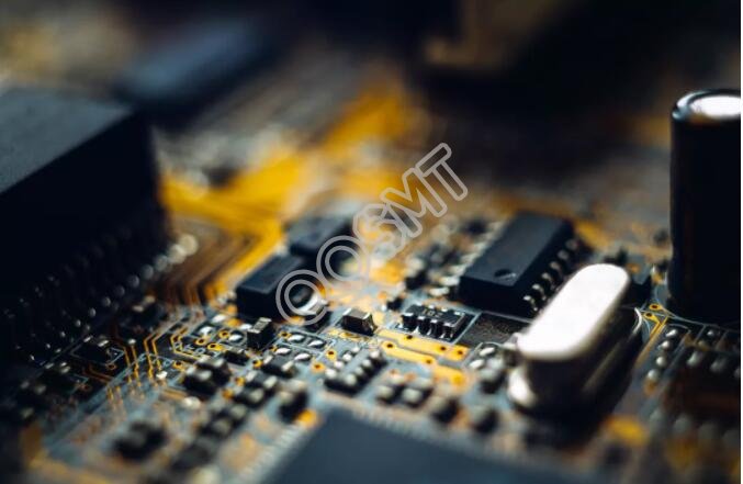
The electronic components have been redesigned, the original pins have been shortened or even eliminated, and the volume has become smaller, and then directly soldered to the printed circuit board (Printed Circuit Board, PCB) or other substrate surface by reflow soldering or dip soldering. superior. Such small metal pieces or end caps are called Surface Mounted Devices (SMD).
The difference between SMT and THT component mounting and welding methods is shown in the figure.
The evolution process of THT plug-in process and SMT patch process
02 Common defects and solutions in SMT dispensing process
Component shift
The phenomenon is that the components are displaced after the patch glue is cured, and the component pins are not on the pads in severe cases. The reason is that the amount of glue produced by the patch glue is uneven. For example, the two-point glue for chip components is more than one and the other is less; the component shifts during the placement or the initial adhesion of the patch glue is low; the PCB is placed for too long after the glue is half the glue Curing.
Solution: Check whether the glue nozzle is blocked and eliminate uneven glue; adjust the working state of the placement machine; change the glue; the PCB placement time after dispensing should not be too long (less than 4h).
Will drop after wave soldering
The phenomenon is that the bonding strength of the components after curing is not enough, which is lower than the specified value, and sometimes there will be chipping when touched by hand. The reason is that the curing process parameters are not in place, especially the temperature is not enough, the component size is too large, and the heat absorption is large; the light curing lamp is aging; the amount of glue is not enough; the component/PCB is polluted.
Solution: Adjust the curing curve, especially increase the curing temperature. Usually the peak curing temperature of the thermal curing adhesive is about 150 ℃. Failure to reach the peak temperature will easily cause the chip to fall. For light curing adhesives, it should be observed whether the light curing lamp is aging, whether the lamp tube is blackened; the quantity of glue and whether the components/PCB are polluted are all issues that should be considered.
Floating/shifting of component pins after curing
The phenomenon of this failure is that the component pins float or shift after solidification, and the tin material will enter under the pad after wave soldering. In severe cases, there will be a short circuit or an open circuit. The main causes are uneven patch glue, excessive patch glue, or component deviation during patching.
Solution: adjust the dispensing process parameters; control the dispensing volume; adjust the patch process parameters.
Solder paste printing and chip quality analysis
Analysis of solder paste printing quality
Common quality problems caused by poor solder paste printing are as follows:
① Insufficient solder paste (partially missing or even missing) will result in insufficient solder joints of components after soldering, components open circuits, components offset, and components stand up.
② The adhesion of solder paste will cause the circuit to be short-circuited and the components to deviate after soldering.
③The overall deviation of solder paste printing will lead to poor soldering of the entire board components, such as less tin, open circuit, deviation, vertical parts, etc.
④, the tip of the solder paste is easy to cause a short circuit after soldering.
Main factors leading to insufficient solder paste
When the printing press was working, the solder paste was not added in time.
The quality of the solder paste is abnormal, and foreign objects such as lumps are mixed in it.
The solder paste that has not been used up has expired and has been used a second time.
The quality of the circuit board is inconspicuous, such as the solder resist (green oil) printed on the pad.
The fixed clamping of the circuit board in the printing machine is loose.
The thickness of the solder paste is not uniform.
The solder paste is missing the stencil or there are contaminants on the circuit board (such as PCB packaging, stencil wiping paper, foreign matter floating in the ambient air, etc.).
The solder paste scraper is damaged and the stencil is damaged.
The equipment parameters such as the pressure, angle, speed and demolding speed of the solder paste scraper are not set properly.
After the solder paste was printed, it was accidentally knocked off due to human factors.
The main factors causing solder paste adhesion
The design defect of the circuit board, the pad spacing is too small.
The stencil problem, the hole position is not correct.
The screen is not wiped clean.
The stencil problem causes the solder paste to fall off badly.
The solder paste has poor performance, unqualified viscosity and collapse.
The fixed clamping of the circuit board in the printing machine is loose.
The equipment parameters such as the pressure, angle, speed and demolding speed of the solder paste scraper are not set properly.
After the solder paste is printed, it is squeezed and adhered due to human factors.
The main factors leading to the overall deviation of solder paste printing
The positioning reference point on the circuit board is not clear.
The positioning reference point on the circuit board is not aligned with the reference point of the screen board.
The fixed clamping of the circuit board in the printing machine is loose. The positioning thimble is not in place.
The optical positioning system of the printing press is malfunctioning.
The solder paste is not printed with the openings of the stencil and the design documents of the circuit board are not in conformity.
The main factors leading to the sharpening of printed solder paste
There is a problem with performance parameters such as solder paste viscosity.
There is a problem with the demoulding parameter setting when the circuit board is separated from the missing screen.
There are burrs on the hole wall of the stencil hole.
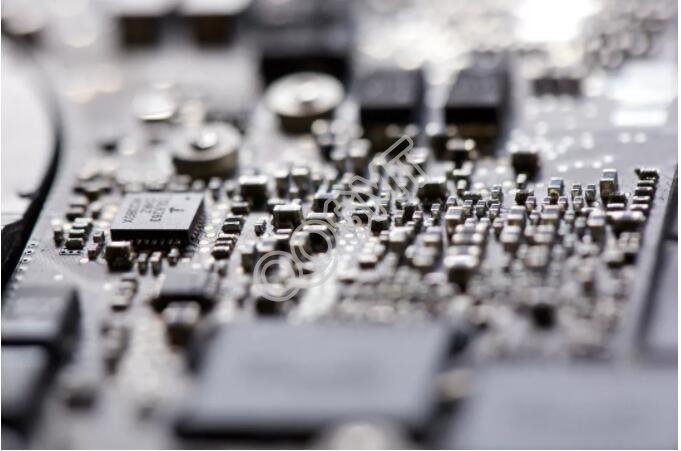
SMT patch quality analysis
Common quality problems of SMT patch include missing parts, side parts, flipped parts, offset, damaged parts, etc.
The main factors leading to missing parts of the patch
The component feeder is not feeding properly.
The air path of the component suction nozzle is blocked, the suction nozzle is damaged, and the suction nozzle height is incorrect.
The vacuum circuit of the equipment is faulty and blocked.
The circuit board is poorly purchased and deformed.
There is no solder paste or too little solder paste on the pads of the circuit board.
The quality of the components is inconsistent, and the thickness of the same product is inconsistent.
The placement machine call program has errors or omissions, or the component thickness parameters are selected incorrectly during programming.
The main factors that lead to the overturning and side pieces of SMC resistors
Abnormal feeding of the component feeder.
The height of the nozzle of the placement head is incorrect.
The height of the pick-up head is wrong.
The size of the loading hole of the component tape is too large, and the component is turned over due to vibration.
The direction of the bulk material was reversed when it was put into the braid.
The main factors leading to component placement deviation
When programming the placement machine, the X-Y axis coordinates of the components are incorrect.
The suction nozzle of the patch makes the suction unstable.
The main factors that cause damage to components during placement
The positioning thimble is too high, so that the position of the circuit board is too high, and the components are squeezed during mounting.
When programming the placement machine, the Z-axis coordinates of the components are incorrect.
The nozzle spring of the placement head is stuck.
Factors affecting the quality of SMT reflow soldering
Influencing factors of solder paste
The quality of reflow soldering is affected by many factors. The more important factors are the temperature profile of the reflow soldering furnace and the composition parameters of the solder paste. Now the commonly used high-performance reflow soldering furnace can accurately control and adjust the temperature curve more conveniently. In contrast, in the trend of high density and miniaturization, the printing of solder paste has become the key to the quality of reflow soldering.
The particle shape of the solder paste alloy powder is related to the soldering quality of narrow-pitch devices, and the viscosity and composition of the solder paste must also be selected appropriately. In addition, solder paste is generally stored in refrigeration. When taking it, it can only be opened after it returns to room temperature. Special attention should be paid to avoid mixing the solder paste with moisture due to temperature differences. If necessary, use a mixer to stir the solder paste evenly.
Influence of welding equipment
Sometimes, excessive vibration of the conveyor belt of the reflow welding equipment is also one of the factors that affect the welding quality.
Influence of reflow soldering process
After eliminating the quality abnormalities of the solder paste printing process and the placement process, the reflow soldering process itself will also cause the following quality abnormalities:
① Cold welding is usually the reflow welding temperature is low or the time in the reflow zone is insufficient.
② The temperature rise in the preheating zone of the tin bead is too fast (generally required, the slope of the temperature rise is less than 3 degrees per second).
③. The circuit board or components with tin connection are damp, and excessive water content may cause tin explosion to produce tin connection.
④. Cracks are generally caused by excessively rapid temperature drop in the cooling zone (generally, the temperature drop slope of lead soldering is less than 4 degrees per second).
SMT soldering quality defects-reflow soldering quality defects and solutions
In reflow soldering of tombstone phenomenon, chip components often stand up. The reason: the root cause of tombstone phenomenon is that the wetting force on both sides of the component is unbalanced, so the torque at both ends of the component is not balanced, thus Lead to the occurrence of tombstone phenomenon.
The following conditions will cause the wetting force on both sides of the component to be unbalanced during reflow soldering:
(1) The pad design and layout are unreasonable. If the pad design and layout have the following defects, it will cause the wetting force on both sides of the component to be unbalanced.
One of the pads on both sides of the component is connected to the ground or the area of one pad is too large, and the heat capacity at both ends of the pad is uneven.
The temperature difference across the PCB surface is too large to cause uneven heat absorption on both sides of the component pad.
Large-scale devices QFP, BGA, and small chip component pads around the heat sink will have temperature unevenness at both ends.
Solution: Change the pad design and layout
(2) There are problems with solder paste and solder paste printing. The activity of the solder paste is not high or the solderability of the component is poor. After the solder paste is melted, the surface tension is different, which will cause the pad wetting force to be unbalanced. The amount of solder paste printed on the two pads is uneven, and the more side will absorb more heat due to the solder paste, and the melting time will lag, resulting in unbalanced wetting force.
Solution: Choose a solder paste with higher activity to improve the solder paste printing parameters, especially the window size of the template.
(3) The uneven force in the Z-axis direction of the patch shift will cause the uneven depth of the component immersed in the solder paste, and the wetting force on both sides will be unbalanced due to the time difference during melting. If the component patch shifts, it will directly lead to the tombstone.
Solution: Adjust the process parameters of the placement machine.
(4) Incorrect furnace temperature curve. If the furnace body of the reflow soldering furnace is too short and the temperature zone is small, the working curve of the PCB heating will be incorrect, and the wet difference on the board surface will be too large, which will cause the wetting force to be unbalanced.
Solution: Adjust the appropriate temperature curve according to each different product.
(5) The oxygen concentration in nitrogen reflow soldering will increase the wetting power of the solder by using nitrogen protection reflow soldering, but more and more examples show that the phenomenon of tombstone tombstones increases when the oxygen content is too low; usually It is considered that the oxygen content should be controlled to the minus 6th power of (100~500)×10.
Tin beads
Tin bead is one of the common defects in reflow soldering. It not only affects the appearance but also causes bridging. Tin beads can be divided into two types. One type appears on one side of the chip component, often in the shape of an independent large ball; the other type appears around the IC pins and is in the shape of scattered small beads. There are many reasons for the production of tin beads, and the analysis is as follows:
(1) The temperature curve is incorrect. The reflow welding curve can be divided into 4 sections, namely preheating, heat preservation, reflow and cooling. The purpose of preheating and heat preservation is to increase the surface temperature of the PCB to 150°C within 60-90s and keep it warm for about 90s. This not only reduces the thermal shock of the PCB and components, but also ensures that the solvent of the solder paste can be partially volatilized. Avoid splashing caused by too much solvent during reflow soldering, causing the solder paste to rush out of the pad and form tin beads.
Solution: Pay attention to the heating rate, and adopt a moderate preheating, so that there is a good platform to make most of the solvent volatilize.
(2) The quality of solder paste
The metal content in the solder paste is usually (90±0.5)℅. Too low metal content will cause too much flux. Therefore, too much flux will cause flying beads due to the fact that the preheating stage is not easy to volatilize.
Increased water vapor and oxygen content in solder paste can also cause flying beads. Since solder paste is usually refrigerated, when it is taken out of the refrigerator, if the recovery time is not ensured, water vapor will enter; in addition, the lid of the solder paste bottle must be tightly closed after each use. If it is not tightly closed in time, it will also cause water vapor. Entry of steam.
After the solder paste printed on the template is completed, the remaining part should be treated separately. If it is put back in the original bottle, the solder paste in the bottle will deteriorate and tin beads will also be produced.
Solution: Choose high-quality solder paste and pay attention to the storage and use requirements of solder paste.
(3) Printing and patching
In the solder paste printing process, due to the offset between the template and the pad, if the offset is too large, the solder paste will immerse and flow out of the pad, and solder balls are likely to appear after heating. In addition, the poor printing environment will also lead to the formation of tin beads. The ideal printing environment temperature is 25±3℃ and the relative humidity is 50℅~65℅.
Solution: carefully adjust the clamping of the template to prevent loosening. Improve the printing working environment.
The pressure on the Z axis during the patching process is also an important cause of tin beading, but it often does not attract people's attention. The Z-axis head of some mounters is positioned according to the thickness of the component. If the height of the Z-axis is not adjusted properly, it will cause the solder paste to be squeezed out of the pad when the component is attached to the PCB. This part of the solder paste will Tin beads are formed during soldering. The tin beads produced in this case are slightly larger in size.
Solution: heavyNewly adjust the Z-axis height of the placement machine.
The thickness of the template and the size of the opening. If the thickness of the template and the size of the opening are too large, the amount of solder paste will increase, and it will also cause the solder paste to overflow to the outside of the pad, especially the template manufactured by chemical etching.
Solution: Choose a template with an appropriate thickness and the design of the opening size. Generally, the opening area of the template is 90℅ of the pad size.
Wicking
The wicking phenomenon, also known as the core-pulling phenomenon, is one of the common welding defects, which is more common in gas phase reflow welding. The wicking phenomenon causes the solder to leave the pad and travel along the pin to between the pin and the chip body, which usually results in a serious virtual soldering phenomenon. As long as the cause is due to the high thermal conductivity of the component pins, the temperature rises rapidly, so that the solder preferentially wets the pins. The wetting force between the solder and the pin is much greater than the wetting force between the solder and the pad. In addition, the pin’s The upturning will aggravate the occurrence of wicking.
Solution:
For gas-phase reflow welding, the SMA should be fully preheated first and then put into the gas-phase furnace.
The solderability of PCB pads should be carefully checked. PCBs with poor solderability cannot be used in production.
Pay full attention to the coplanarity of components, and devices with poor coplanarity cannot be used in production.
In infrared reflow soldering, the organic flux in the PCB substrate and solder is a good infrared absorbing medium, while the pins can partially reflect infrared. Therefore, the solder is preferentially melted, and the wetting power of the solder and the pad is limited. Will be greater than the wetting force between the solder and the lead, so the solder will not rise along the lead, so the probability of wicking is much smaller.
Bridging
Bridging-is one of the common defects in SMT production. It can cause short circuits between components. When bridging is encountered, it must be repaired. There are many reasons for bridging:
(1) Quality problems of solder paste
The metal content in the solder paste is too high, especially if the printing time is too long, the metal content is likely to increase, leading to bridging of IC pins.
The solder paste has a low viscosity and flows out of the pad after preheating.
The solder paste tower has a poor drop and overflows to the outside of the pad after preheating.
Solution: Adjust the solder paste ratio or switch to good quality solder paste.
(2) Printing system
The printer has poor repeat accuracy and misalignment (bad steel plate alignment, poor PCB alignment), causing solder paste to be printed outside the pads, especially fine-pitch QFP pads.
The size and thickness of the template window are not designed correctly, and the Sn-pb alloy coating of the PCB pad design is not uniform, resulting in a large amount of solder paste.
Solution: Adjust the printer to improve the coating layer of the PCB pad.
(3) Excessive placement pressure and full flow of solder paste after pressure are common reasons in production. In addition, insufficient placement accuracy will cause component displacement and IC pin deformation.
(4) The heating rate of the reflow soldering furnace is too fast, and the solvent in the solder paste is too late to volatilize.
Solution: Adjust the height of the Z axis of the placement machine and the heating rate of the reflow soldering furnace.
Wave soldering quality defects and solutions
(1) Sharpening refers to the appearance of excess needle-like solder at the end of the solder joint, which is a unique defect in the wave soldering process.
Causes: Improper PCB transmission speed, low preheating temperature, low tin pot temperature, small PCB transmission inclination, poor wave crest, flux failure, and poor solderability of component leads.
Solution: Adjust the transmission speed until it is appropriate, adjust the preheating temperature and tin pot temperature, adjust the PCB transmission angle, optimize the nozzle, adjust the wave shape, exchange the new flux and solve the lead solderability problem.
Recommended setting values for each section of the reflow temperature curve:
①Normal temperature~starting point of preheating
Image
②Preheating zone
Image
Excessive preheating leads to deepening of oxidation and deterioration of flux
③The end of preheating ~ reflow soldering area
④Reflow soldering area ~ cooling area
The peak temperature of SMT reflow soldering usually depends on the melting point temperature of the solder and the temperature that the assembled parts can withstand. The first thing to consider is whether your components, and PCB boards, can withstand this temperature, because the composition of lead solder paste and lead-free is different. The composition of lead is: tin: 63%, lead: 37%, and the melting point is generally 183. The peak value is 205-230 and the lead-free ones are: tin 96.5%; silver: 3%; copper: 0.5%, so the high melting point is generally: 217, the peak value is: 245---250; the general peak temperature should be higher than tin The normal melting point temperature of the paste must be about 25~30°C higher in order to successfully complete the soldering operation. If it is lower than this temperature, it may cause the disadvantages of cold welding and poor wetting.
(2) Causes of false soldering: poor solderability of component leads, low preheating temperature, solder problems, low flux activity, large pad holes, oxidation of the lead board, contamination on the board, excessive transmission speed, tin The pot temperature is low.
Solution: Solve the solderability of the lead, adjust the preheating temperature, test the tin and impurity content of the solder, adjust the flux density, reduce the pad hole during the design, remove the PCB oxide, clean the board surface, adjust the transmission speed, adjust the tin pot temperature .
(3) Causes of thin tin: poor solderability of component leads, large pads (except for large pads), large pad holes, large soldering angles, excessive transmission speed, high tin pot temperature, and flux Uneven coating and insufficient tin content in solder.
Solution: Solve the solderability of the lead, reduce the pads and pad holes during the design, reduce the welding angle, adjust the transmission speed, adjust the temperature of the tin pot, check the pre-coated flux device, and test the solder content.
(4) Causes of missing soldering: poor lead solderability, unstable solder wave, flux failure or uneven spraying, poor local solderability of PCB, transmission chain jitter, pre-coated flux and flux are incompatible, and the process flow is unreasonable .
Solution: Solve the lead solderability, check the wave device, replace the flux, check the pre-applied flux device, solve the PCB solderability (cleaning or return), check and adjust the transmission device, use the flux uniformly, and adjust the process flow.
(5) Blistering of the solder mask on the printed board after soldering
SMA will appear light green bubbles around individual solder joints after welding. In severe cases, nail cap-sized bubbles will appear, which not only affects the appearance quality, but also affects performance in severe cases. This defect is also a reflow welding process. The problem often occurs in the middle, but the wave soldering time is more.
Cause: The root cause of the solder mask blistering is the presence of gas or water vapor between the solder mask and the PCB substrate. These trace amounts of gas or water vapor will be entrained in it during different processes. When the soldering high temperature is encountered , The gas expansion causes the delamination between the solder mask and the PCB substrate. During soldering, the temperature of the pad is relatively high, so bubbles first appear around the pad.
One of the following reasons can cause moisture to be entrained on the PCB
(1) PCBs often need to be cleaned and dried during the processing process before proceeding to the next process. For example, the solder mask should be dried after being etched. If the drying temperature is not enough at this time, moisture will be entrained into the next process. Air bubbles appear when welding at high temperature.
(2) The storage environment before PCB processing is not good, the humidity is too high, and it is not dried in time during soldering.
(3) In the wave soldering process, water-containing flux is often used now. If the PCB preheating temperature is not enough, the water vapor in the flux will enter the inside of the PCB substrate along the hole wall of the through hole, and the pad will enter first Water vapor will produce bubbles after encountering welding high temperature.
(4) Strictly control all production links. The purchased PCB should be put into the warehouse after inspection. Usually, the PCB should not blistering within 10s at a temperature of 260°C.
(5) PCB should be stored in a ventilated and dry environment, and the storage period should not exceed 6 months.
(6) The PCB should be pre-baked in an oven at (120±5)℃ for 4 hours before soldering.
(7) The preheating temperature in wave soldering should be strictly controlled. It should reach 100-140℃ before entering wave soldering. If water-containing flux is used, the preheating temperature should reach 110-145℃ to ensure that the water vapor can be completely volatilized.
Foaming on PCB substrate after SMA soldering
Nail-sized bubbles appear after SMA welding, the main reason is the moisture entrained inside the PCB substrate, especially the processing of multi-layer boards. Because the multi-layer board is pre-formed by multiple epoxy resin prepregs and then hot pressed, if the storage period of the epoxy resin prepregs is too short, the resin content is not enough, and the pre-drying to remove water vapor is not clean, it will be easy to form after hot pressing. Entrained water vapor. The semi-solid sheet itself may also have insufficient glue content and insufficient bonding force between the layers, leaving air bubbles. In addition, after the PCB is purchased, due to the long storage period and humid storage environment, there is no timely pre-baking before the patch production, and the damp PCB is also prone to blistering after the patch.
Solution: After the PCB is purchased, it should be checked and accepted before being put into the warehouse. The PCB should be pre-baked at (120±5)℃ for 4 hours before mounting.
IC pins are open or soldered after soldering
cause:
Poor coplanarity, especially FQFP devices, lead to deformation due to improper storage. If the placement machine does not have the function of checking coplanarity, it is sometimes difficult to find.
Poor solderability of the pins, long IC storage time, yellowing of the pins, and poor solderability are the main causes of false soldering.
The solder paste is of poor quality, low metal content, and poor solderability. The solder paste usually used for soldering FQFP devices should have a metal content of not less than 90%.
If the preheating temperature is too high, it is easy to cause oxidation of the IC pins and worsen the solderability.
The size of the printing template window is so small that the amount of solder paste is insufficient.
Pay attention to the custody of the device, do not take the component or open the package casually.
The solderability of the components should be checked during production, and special attention should be paid to the IC storage period should not be too long (within one year from the date of manufacture), and the storage should be protected from high temperature and high humidity.
Carefully check the size of the template window, it should not be too large or too small, and pay attention to matching the size of the PCB pad.