Another problem occurs during BGA device welding process?
Jan 12, 2024
test analysis
During the assembly process of a certain model of BGA, there is a certain proportion of tin connections that fail, and the positions of the tin connections are relatively fixed.
Now test and analyze the failed PCBA, BGA raw materials, PCB bare board, normal PCBA and PCBA semi-finished product (after the first side reflow soldering) to find the cause of the failure.
test analysis
1. Appearance inspection
The structure of the failed PCBA had no obvious deformation, the structure of the problematic BGA device was intact, and no obvious abnormalities were found.
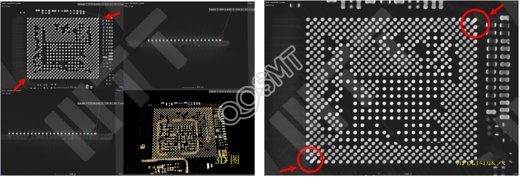
2. CT tomography analysis
A comprehensive scan and analysis of the BGA device was carried out through CT three-dimensional imaging technology. The results are as follows:
①The tin connection is mainly concentrated at both ends of one of the diagonal lines of the device;
②In the diagonal direction of tin connection failure, the solder joint gap is significantly smaller than in other directions.
The above phenomenon infers that the BGA is severely deformed in the diagonal direction of failure and is in a squeezed state.
Figure 1. CT tomography results
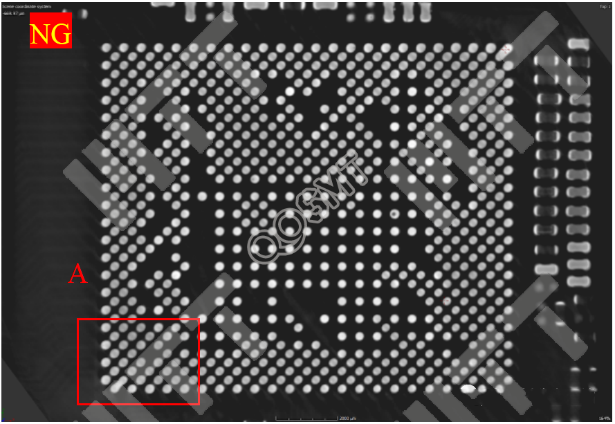
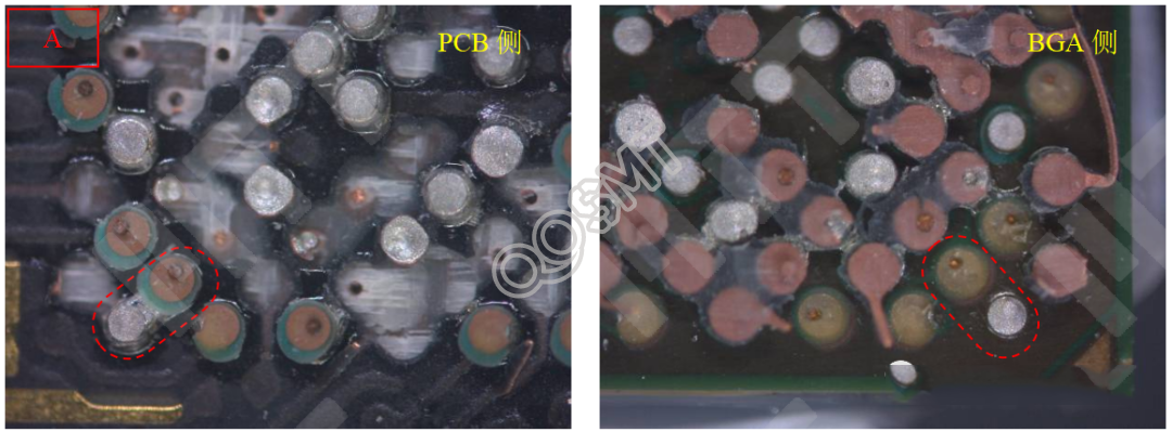
3. Peel-off analysis
The failed BGA was observed after mechanical peeling, and it was found that there were two tin connections at the diagonal edges, which was consistent with the X-Ray observation results. The solder and PCB surface at the connection point are completely non-moisturizing.
When wet, the contact surface shows an extruded morphology, which can rule out the possibility of tin connection caused by abnormal surface energy of the green oil.
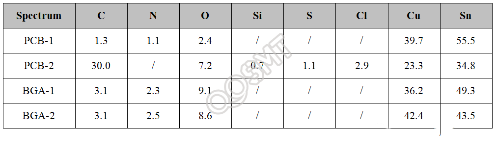
As shown in Figure 2, Figure 3 and Table 1-2, no abnormal elements were found at the solder joints, and the morphological characteristics are completely consistent with Figure 1.
Figure 2. Photo after peeling off the failed BGA
Table 1. Surface composition test results of failed BGA after peeling off (wt.%)
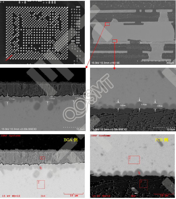
4. Profile analysis
4.1 Analysis of connected tin slices
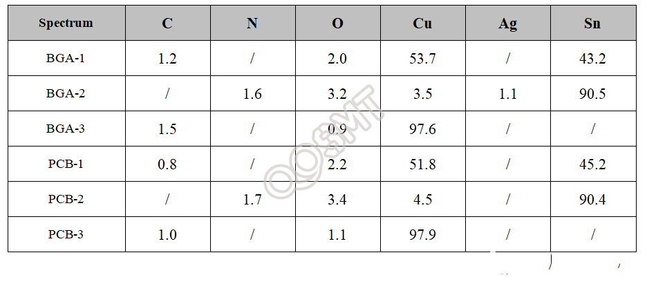
SEM/EDS analysis was performed after slicing the failed BGA. The IMC thickness of the solder joints was normal, indicating that the welding heat input was normal. The solder in the tin connection part is in complete contact with the PCB solder mask without any gaps.
, this phenomenon indicates that there is too much printing solder paste or excessive thermal deformation during the process.
Figure 4. SEM picture of failed BGA cross-section
Table 2. Failed BGA profile composition test results (wt.%)
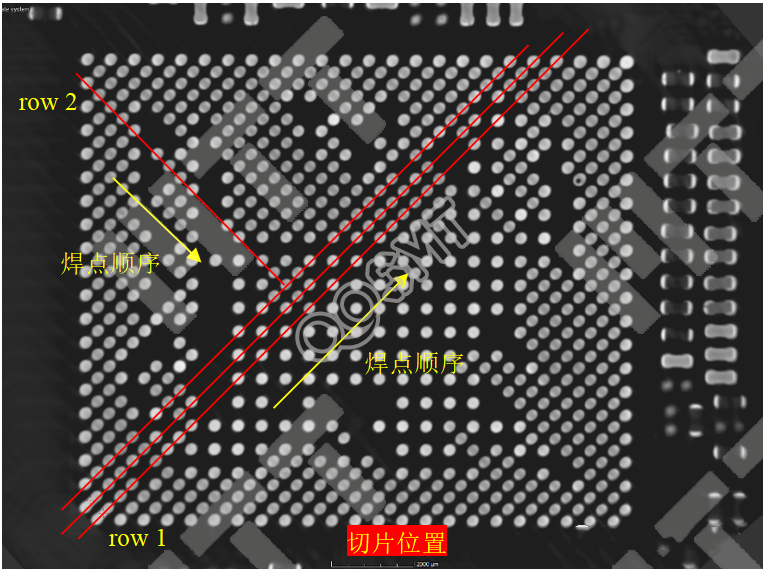
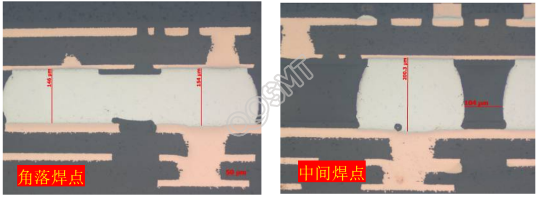
4.2 Statistical analysis of solder joint height
In order to confirm the degree of compression deformation of the corners, the data statistics of the height of the solder joints and the gap between the solder joints in the two diagonal directions were carried out through slice measurement. The results are as follows:
Failed BGA:
ROW1: The overall trend is that the height of the solder joints on both sides is small and the height of the middle solder joint is large. The minimum solder joint height is 146um and the maximum is 201.3um, with a difference of 55.3um. The solder joint gap is small and medium at the edge
The general trend is that the minimum is 50.8um and the maximum is 102.7um;
ROW2 (only half length diagonal): The overall trend is that the height of the solder joints on both sides is small and the height of the middle solder joint is large. The minimum solder joint height is 162.1um and the maximum is 190.9um, with a difference of 28.8um.
. The solder joint gap shows a trend of small edges and large middle, with a minimum of 76.1um and a maximum of 118um.
The reduction in solder joint height is the most direct cause of tin connection failure.
Figure 5. Failed BGA slice position, solder joint height, and solder joint gap statistical chart
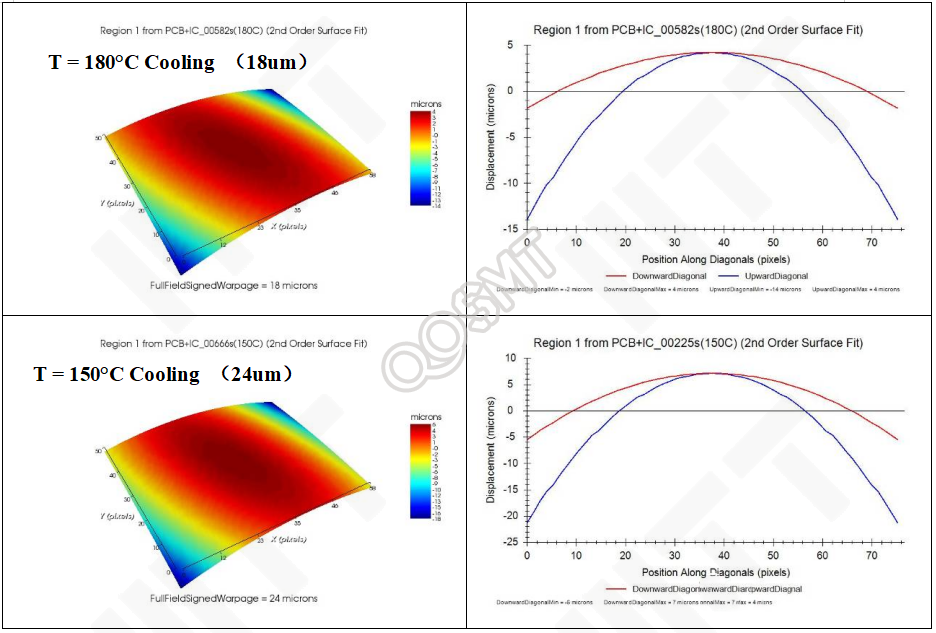
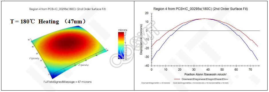
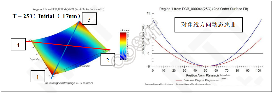
5. Warpage analysis
In order to confirm the degree of diagonal deformation of the material during the reflow process, the Shadow moiré equipment was used to test the dynamic warpage.
PCB: Both the whole bodies show convex deformation. The maximum deformation is found on the 1-3 diagonal (failure diagonal), which occurs at 150℃ and 180℃ respectively in the heating stage. The deformation amount is
28um and 24um.
BGA: Both the whole parts show convex deformation (when the solder ball is placed downward, the whole device shows concave deformation), and the maximum deformation is found on the 2-4 diagonal lines, which occur during the cooling stage.
At 222℃ and 180℃ in the heating stage, the deformation amounts are 42um and 47um. The thermal deformation of this BGA device meets the requirements.
PCBA semi-finished product: The overall display shows concave deformation, and the deformation of diagonal lines 1-3 is more significant, which is consistent with the actual slicing results.
The dynamic warpage test results show that the overall concave deformation of the PCBA semi-finished product occurs during the welding process, and the concave deformation in the diagonal direction of failure is more obvious, which is consistent with the actual deformation trend after welding.
6 Conclusion
The fundamental reason why the BGA is soldered at a relatively fixed position: During the soldering process of the PCBA semi-finished product (first side reflow soldering), a large degree of concave deformation occurs in the fixed diagonal direction, resulting in
The solder joints at the corners are squeezed and connected to the tin.