Before soldering the plug-in, it was found that the PCB pad was "blackened".
Jan 12, 2024
Two days after the reflow soldering of a certain PCB patch, the PCB pad was found to be "blackened" before the plug-in was soldered. Test and analyze the PCB to find the cause of the "blackening" of the pad.
test analysis
1. Failure confirmation
Conduct a visual inspection of the NG PCB to confirm the failure phenomenon, and compare it with the unbaked board. It is found that the color of the NG pad is obviously darker, that is, the pad is "black" and the surface is rough.
It has a blocky shape; while the surface of the unpaved PCB pad is brownish yellow, relatively flat, and has no obvious abnormal features.
2. Pad surface analysis
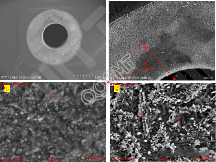
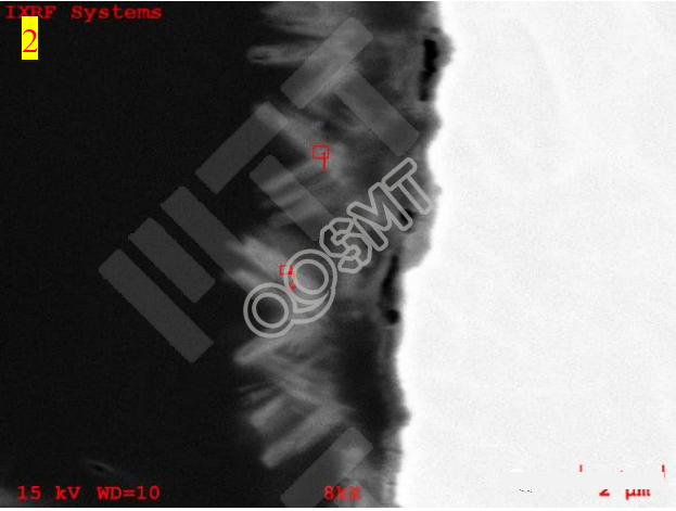
Surface analysis of NG pads and unbaked boards revealed that there are two types of morphologies on the surface of NG PCB: ① Obvious film-like covering with a high Cl content of about 11.4wt%; ② Corrosion
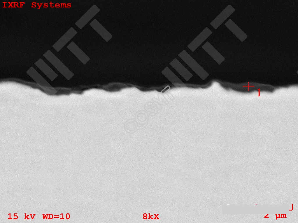
Corroded crystalline morphology, Cl content is also high, about 14.7wt%, as shown in Figure 1, Table 1; while the surface of the unpaved pad is relatively smooth, and no obvious corrosion morphology is found; the surface of the pad is mainly formed
Divided into C, O, Cl, and Cu, the Cl content is 1.1wt.%~5.6wt.%, as shown in Figure 2 and Table 2.
Figure 1. SEM picture and EDS spectrum of NG pad surface
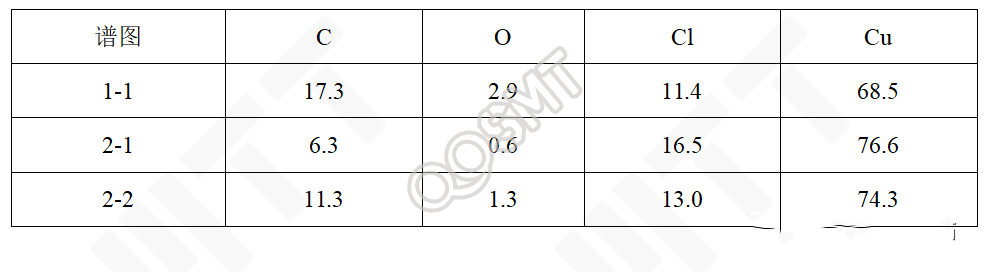
Table 1. NG pad surface EDS results (Wt.%)
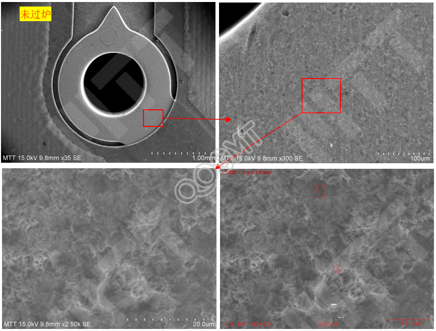
Figure 2. SEM picture of the unpaved pad surface
3. Pad profile analysis
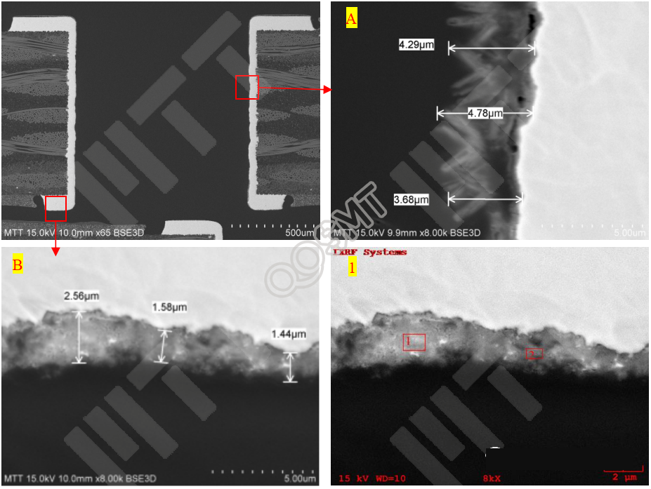
Conduct cross-section analysis on NG PCB and unbaked board pads. As shown in Figure 3 and Table 3, the OSP film on the surface of the pad in area A of NG PCB is crystalline with a thickness of 3.68~4.29μm; NG PCB B
The OSP film on the area pad is foggy, with a thickness of 1.44~2.58μm; the main components of the OSP film in each area are C, O, Cl, and Cu, and the contents of Cl and Cu are relatively high, ranging from 6.8 wt.% to 16.8wt respectively. %
, 41.7wt.%~73.3wt.%.
Figure 3. SEM picture of NG PCB pad cross-section
As shown in Figure 4 and Table 4, the OSP film of the unpaved pad has uniform contrast, no obvious impurities, and a thickness of approximately 0.68~1.26μm. The main components of the OSP film are C, O, Cl, and Cu, of which the Cu content is
7.9wt.%, Cl content is 3.9wt.%.
From the above test results, it can be seen that the NG PCB OSP film has obvious corrosion morphology, which is mainly related to the corrosion of the bottom copper; there is a huge difference between the OK PCB OSP film and the NG PCB. The main difference between the two
Reflected in bottom copper corrosion.
Figure 4. SEM picture of the unheated PCB pad cross-section
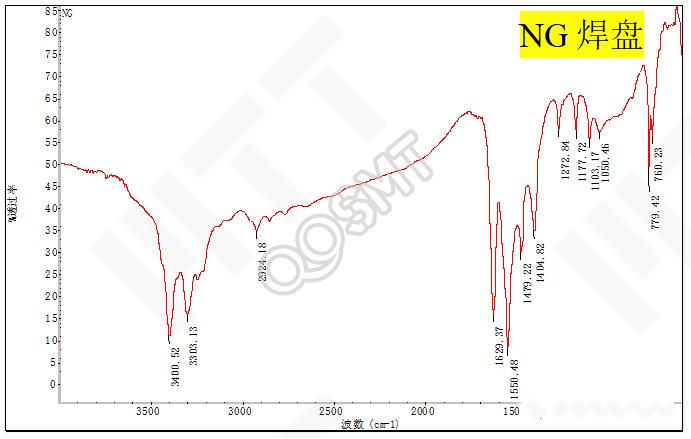
4. FT-IR analysis
Infrared analysis of the failed PCB pad surface revealed that the main component of the NG pad surface was amide compounds, while the main component of the OSP film-forming material was chlorobenzimidazole derivatives.
Figure 5. FTIR infrared spectrum spectrum
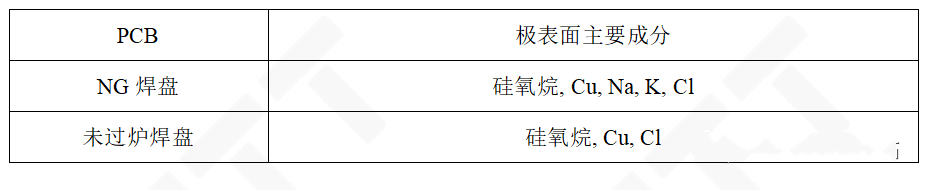
5. TOF-SIMS extreme surface composition analysis
TOF-SIMS was used to conduct composition analysis on the surface of NG PCB and unfired PCB pads. Through comparison, it was found that there are a large number of Na and K abnormal elements on the surface of NG pads, indicating that the surface of NG pads
There is pollution on the surface. Combined with the analysis of EDS test results, Na and K abnormal elements only exist on the surface of the pad and have no direct correlation with the corrosion of the bottom copper.
Table 6.TOF-SIMS test results
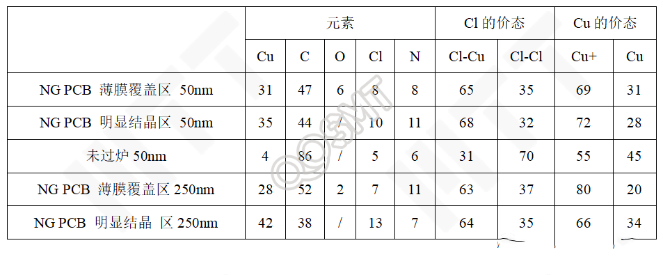
6. XPS in-depth component analysis
Use XPS to analyze the components in the longitudinal direction of the NG PCB pad surface (analyze the film coverage area and obvious crystallization area in Figure 1 respectively), and compare it with the unfired PCB. The results are as follows:
①At a depth of 50nm from the pad surface, there is no essential difference in the composition of NG PCB and unpaved PCB. NG PCB has relatively high Cu and Cl element content, and Cu and Cl elements mainly exist in ionic state.
; The Cl element of unfired PCB is mainly covalent bond, which is consistent with the surface corrosion crystal morphology.
② At a depth of 250nm from the pad surface, the changes in different areas of the NG PCB are slightly different, and Cu and Cl elements still mainly exist in ionic states.
Table 7.XPS test results (At%)
in conclusion
The "blackening" of the pad during the OSP pad assembly process is caused by the corrosion and crystallization of the bottom copper, which is directly related to the high Cl element content and the lack of control during the circulation and storage process.