Selection and use of SMT components
Jan 20, 2024
1. Assembly adaptability - to adapt to various assembly equipment operations and process flows
2. Welding adaptability - to adapt to various welding equipment and related processes
2. Selection of SMT components
3. Precautions when using SMT components
2. Storage cycle of components
3. Requirements when taking SMT components
4. How to save remaining SMD
4. Development of SMT device packaging forms
2. Multi-chip module (MCM) technology
3. Three-dimensional assembly technology
1. Basic requirements for SMT components
SMT components should meet the following basic requirements.
1. Assembly adaptability - to adapt to various assembly equipment operations and process flows
(1) SMT components must be placed on the circuit board using a placement machine before welding. Therefore, the upper surface of the components should be suitable for picking up by the vacuum nozzle of the placement machine.
(2) Space for adhesive should be reserved on the lower surface of SMT components (excluding solder terminals).
(3) The size and shape should be standardized and have good dimensional accuracy and interchangeability.
(4) The packaging form is suitable for automatic placement by the placement machine, and can protect the device from external forces during transportation and keep the pins flat.
(5) It has a certain mechanical strength and can withstand the mounting stress and the bending stress of the circuit substrate.
2. Welding adaptability - to adapt to various welding equipment and related processes
(1) The soldering terminals or pins of components have good coplanarity and meet mounting and welding requirements.
(2) The materials and packaging of components have good high temperature resistance and are suitable for welding conditions:
●Reflow soldering (235±5)℃, soldering time (5±0.2)s.
● Wave soldering (250±5)℃, soldering time (4±0.5)s.
(3) It can withstand cleaning with organic solvents after welding, and the packaging materials and surface markings must not be dissolved.
2. Selection of SMT components
When selecting SMT components, factors such as specifications, performance, and price that market suppliers can provide should be considered based on system and circuit requirements.
(1) When selecting components, pay attention to the placement accuracy level of the placement machine.
(2) Tantalum and aluminum electrolytic capacitors are mainly used in situations with large capacitance. Aluminum electrolytic capacitors have large capacity, high withstand voltage and are relatively cheap, but the pins are under the base and the reliability of welding is not as good as that of rectangular packaged tantalum electrolytic capacitors.
(3) The pin form of the integrated circuit is related to the welding equipment and working conditions, and is an issue that must be considered. Although the typical soldering method for SMT is reflow soldering, chips with a small number of wing-shaped pins can also be placed on the soldering surface of the circuit board and soldered with wave soldering equipment. Experienced technical workers can use a hot air table or even an ordinary electric soldering iron. Can also be skillfully welded. J-shaped pins are not easily deformed. For integrated circuits such as single-chip computers or programmable memories that need to be disassembled multiple times to erase and write their internal programs, PLCC-encapsulated chips are matched with special sockets to make disassembly or replacement easy. But if the product has been mass-produced, reducing the number of PLCC sockets can obviously reduce costs; however, PLCC chips directly soldered to the circuit board are not convenient to repair, and wave soldering equipment cannot be used for soldering. Spherical pins are the development direction of large-scale integrated circuits, but BGA integrated circuits certainly cannot use wave soldering or manual soldering.
(4) Most electromechanical components are made of plastic skeletons, which are easily deformed by heat during welding. It is best to use electromechanical components with exposed pins.
3. Precautions when using SMT components
1. Environmental conditions for storage of SMT components
● Ambient temperature: Stock temperature <40℃.
● The temperature at the production site is <30℃.
●Ambient humidity: <RH60%.
● Environmental atmosphere: There should be no toxic gases such as sulfur, chlorine, acid, etc. that affect the welding performance in the storage and use environment.
● Anti-static measures: Meet the anti-static requirements of SMT components.
2. Storage cycle of components
Calculated from the production date of the component manufacturer, the inventory time does not exceed 2 years; the inventory time after purchase by the complete machine factory user generally does not exceed 1 year; if it is a complete machine factory with a relatively humid natural environment, SMT components should be purchased after purchase. Use within 3 months, and take appropriate moisture-proof measures in the storage location and component packaging.
SMD devices with moisture-proof requirements: must be used within 72 hours after opening, and no longer than one week. If it cannot be used up, it should be stored in a drying oven with RH20%. SMD devices that have been dampened should be dried and dehumidified according to regulations.
Things to note when baking:
(1) For SMDs packaged in plastic tubes (SOP, SOJ, PLCC and QFP, etc.), the packaging tubes are not resistant to high temperatures and cannot be placed directly in the oven for baking. They should be placed in a metal tube or metal plate before baking.
(2) QFP packaging plastic trays are available in two types: non-high temperature resistant and high temperature resistant. Those that are resistant to high temperatures (marked with Tmax=135℃, 150℃ or 180℃, etc.) can be directly placed in the oven for baking. Those that are not resistant to high temperatures cannot be directly placed in the oven for baking to prevent accidents and should be placed separately. Bake in a metal pan. When transferring, avoid damaging the pins to avoid damaging their coplanarity.
3. Requirements when taking SMT components
During transportation, material distribution, inspection or manual mounting, if workers need to take SMT devices, they should wear anti-static wrist straps, use suction pens as much as possible, and pay special attention to avoid damaging the pins of SOP, QFP and other devices. Prevent pin warping and deformation.
4. How to save remaining SMD
(1) Equipped with a special low-temperature and low-humidity storage box. Store unused SMDs in the box together with the feeder after opening. However, it is more expensive to equip a large dedicated low-temperature and low-humidity storage box.
(2) Use the original intact packaging bags. As long as the bag is not damaged and the desiccant inside is good (all black circles on the humidity indicator card are blue, no pink), you can still put the unused SMD back into the bag and seal it with tape.
4. Development of SMT device packaging forms
Since its advent in the 1960s, SMT technology has entered a fully mature stage after 50 years of development. It has not only become the mainstream of contemporary circuit assembly technology, but also continues to develop in depth. As far as packaging device assembly processes are concerned, SMT is actively conducting research on multi-chip modules and three-dimensional assembly technology.
1. Chip-level assembly technology
Since the advent of the world's first transistor in 1947, especially with the rapid development of LSI, VLSI and ASIC devices, various advanced IC packaging technologies have emerged, such as DIP, SOP, QFP, BGA and CSP. With the maturity of SMT technology, direct mounting of bare chips onto PCBs has been put on the agenda. In particular, the solution of bottleneck technologies that restrict the development of bare chips, such as PCBs with low expansion coefficients and welding and filling materials, has brought bare chip technology into a new era. A new era of rapid development. The annual growth rate of bare chips has reached more than 30% since 1997. The rapidly developing bare chip applications include computer-related components, such as microprocessors, high-speed memory and hard drives. In addition, there are some portable Equipment, such as mobile phones, digital cameras, etc. In the end, all consumer electronics products will also use bare chip technology extensively due to the development trend of high performance and miniaturization. Therefore, bare chip technology will surely become the mainstream of chip application development in the 21st century.
There are two main forms of bare chip soldering technology: one is COB technology, and the other is flip chip technology FC (Flip Chip).
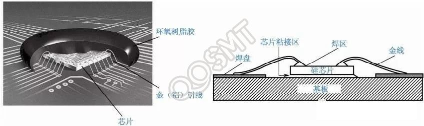
(1) COB method. The COB method uses wire bonding to assemble the bare chip directly on the PCB. The soldering area and the chip body are on the same plane, and the periphery of the soldering area is evenly distributed. The minimum area of the soldering area is 90 μm × 90 μm, and the minimum spacing is 100 μm. , PCB pads have corresponding pad numbers, which are also arranged peripherally.
During welding, first stick the bare chip to the PCB with conductive/thermal conductive adhesive. After solidification, use a wire bonding machine (binding machine) to connect the metal wires (Al or Au) to the chips under the action of ultrasonic and hot pressure. The I/O terminal pads on the PCB and the corresponding pads on the PCB are then encapsulated with epoxy resin to protect the bonding wires. The COB method is shown in Figure 1. COB technology has the advantages of low price, space saving and mature technology. However, the COB method is not suitable for large-volume automatic placement, and the PCB manufacturing process used for the COB method is relatively difficult; in addition, due to certain difficulties in heat dissipation of COB, it is usually only suitable for low power consumption (0.5~1 W) IC chip.
Figure 1 COB method
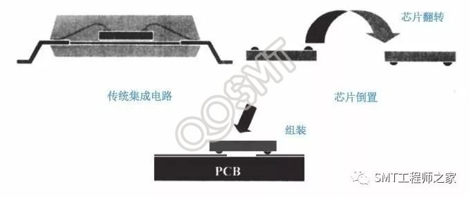
(2) FC method. FC is also called flip chip. Compared with COB, its I/O terminals are arranged on the chip in an area array, and solder bumps are made on the surface of the I/O terminals. When welding, just place the chip upside down on the PCB so that the bumps are aligned with the pads on the PCB. After heating, the interconnection between FC and PCB can be achieved. Therefore, FC can be processed using technical means similar to SMT. The FC process is shown in Figure 2.
Figure 2 FC process
As early as the late 1960s, IBM used FC technology extensively in computers, that is, mounting high-density FCs on ceramic printed boards; by the 1990s, this technology had been used in electronic products in various industries. applications, especially in portable communication devices. IBM calls the process of connecting FC to PCB Controlled Collapse Chip Connection, or C4 for short. During the welding process, the bare chip is affected by the surface tension of the molten solder on the one hand and can correct its position on its own. On the other hand, it is affected by gravity and the chip height decreases to a limited extent. Therefore, whether FC is packaged or welded, its process is reliable and feasible. Currently, this technology has received widespread attention from the electronic assembly industry.
2. Multi-chip module (MCM) technology
MCM is an advanced hybrid integrated circuit that has developed rapidly since the 1990s. It assembles several IC chips on a circuit board to form a functional circuit block, called a multi-chip module (MCM, Multi Chip Module). ).
It can be said that MCM technology is an extension of SMT. The functions of a set of MCMs are equivalent to the functions of a subsystem. Usually the MCM substrate has more than 4 layers of wiring and more than 100 I/O pins, and interconnects CSP, FC, and ASIC devices with it. It represents the essence of electronic assembly technology in the 1990s and is the crystallization of semiconductor integrated circuit technology, thick film/thin film hybrid microelectronics technology, and printed board circuit technology. It is internationally known as Microelectronic Packaging Technology. MCM technology is mainly used in ultra-high-speed computers and outer space electronics technology.
MCM technology is usually divided into three major categories, namely MCM-L, MCM-C, and MCM-D. MCM-L is the production of multi-layer high-density assembly and interconnection on printed circuits. It is an extension and development of COB chip-PCB assembly technology. MCM-C uses thick film and thin film multilayer methods to create high-density assembly and interconnection on ceramic multilayer substrates. MCM-D is a technology that uses deposition methods to produce thin-film multi-layer high-density assembly and interconnection on silicon substrates or other new substrates. It has the highest technical content in MCM production.
If several pieces of MCM are assembled on an ordinary circuit board, electronic equipment or system-level functions can be realized, thereby realizing modularization of military and industrial circuit components. The first 20 years of the 21st century were a period of popularization and application of MCM and transformation of electronic equipment.
3. Three-dimensional assembly technology
The guiding idea of three-dimensional assembly technology (referred to as 3D assembly technology) is to stack IC chips (MCM wafers, WSI large wafer scale integrated wafers) one by one, use the side edges of the chips to interconnect in the vertical direction, and convert the horizontal assembly to the vertical direction. The direction is developing into three-dimensional assembly. The realization of three-dimensional assembly not only makes electronic products denser, but also enables them to have more functions, faster signal transmission, better performance, and higher reliability, while the relative cost of electronic systems will be lower. It is the current silicon chip technology the highest level.
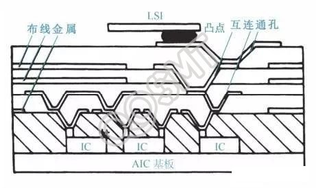
There are currently three ways to achieve 3D assembly: one is to embed R (resistance), C (capacitance) and IC in a multi-layer substrate or multi-layer wiring medium, and then mount various chip components on the top of the substrate, so It is called an embedded 3D structure, as shown in Figure 3; the second is to use it as a substrate after Si wafer scale integration (WSI), perform multi-layer wiring on it, and then mount SMD on the top layer to form a 3D structure. This method is called The active substrate type 3D structure is shown in Figure 4; the third is to interconnect the upper and lower layers of the MCM to form a 3D structure, so it is called a stacked 3D structure, as shown in Figure 5.
Figure 3 Embedded 3D structure
Figure 4 Active substrate type 3D structure
Figure 5 Stacked 3D structure