Detailed explanation of SMT integrated circuit process
Jan 20, 2024
2. Packaging materials
3. How to load the chip
4. Chip substrate type
5.Package ratio
4.LCCC package
5.PQFN packaging
6.BGA package
SMT integrated circuits include SSI~ULSI integrated devices of various digital circuits and analog circuits. Due to the advancement of process technology, the electrical performance indicators of SMT integrated circuits are better than those of THT integrated circuits.
1. Overview of SMT integrated chip packaging
To measure the advancement of integrated circuit manufacturing technology, in addition to the degree of integration (number of gates, maximum number of I/Os), circuit technology, feature size, electrical performance (clock frequency, operating voltage, power consumption), there is also the packaging of the integrated circuit.
The so-called integrated circuit packaging refers to the shell used to install semiconductor integrated circuit chips. It not only plays the role of placing, fixing, sealing, protecting the chip and enhancing the electrothermal performance, but also serves as a bridge between the internal and external circuits of the chip - on the chip. The contacts are connected to the pins of the package shell with wires, and these pins are connected to other components through wires on the printed circuit board. Therefore, packaging plays an important role in integrated circuits. The emergence of a new generation of large-scale integrated circuits is often accompanied by the application of new packaging forms.
1.Electrode form
The I/O electrodes of SMT integrated circuits come in two forms: leadless and leaded. Leadless forms include LCCC, PQFN, etc. After this type of device is mounted, the electrode soldering terminals on the bottom of the chip are directly connected to the pads on the printed circuit board, which has high reliability. The reliability of devices with pins after mounting is related to the shape of the pins, so the shape of the pins is more important. The three dominant pin shapes are wing-shaped, hook-shaped (J-shaped) and ball-shaped. Wing pins are used for SOT/SOP/QFP packages, hook (J-shaped) pins are used for SOJ/PLCC packages, and ball pins are used for BGA/CSP/Flip Chip packages.
The main characteristics of wing-shaped pins are: in line with the development trend of thin and narrow pins and small spacing. It is characterized by easy welding. It can be welded by various welding processes including thermal resistance welding. Process inspection is convenient, but it takes up a lot of space. The area is large and the pins are easily damaged during transportation and loading and unloading.
The main characteristics of the hook pin are: the lead is "J" shaped, and the space utilization rate is higher than that of the wing pin. It can be welded by most reflow soldering methods except thermal resist soldering, and it is stronger than the wing pin. Because the pins have a certain degree of elasticity, they can relieve the stress of installation and welding and prevent solder joints from breaking.
2. Packaging materials
According to the packaging material of the chip, it is divided into metal packaging, ceramic packaging, metal-ceramic packaging and plastic packaging.
(1) Metal packaging: Metal materials can be stamped, so they have the advantages of high packaging precision, strict dimensions, easy mass production, and low price.
(2) Ceramic packaging: Ceramic materials have excellent electrical properties and are suitable for high-density packaging.
(3) Metal-ceramic packaging: It has the advantages of both metal packaging and ceramic packaging.
(4) Plastic packaging: Plastic has strong plasticity, low cost, simple process, and is suitable for mass production.
3. How to load the chip
When a bare chip is loaded, its side with electrodes can be facing up or down. Therefore, the chip can be divided into a regular chip and a flip-chip. The wiring side is facing up for a formal chip, and vice versa.
In addition, when the bare chips are loaded, their electrical connection methods are also different, some use wire bonding, and some use no lead bonding.
4. Chip substrate type
The function of the substrate is to carry and fix the bare chip, and also has the functions of insulation, heat conduction, isolation and protection. It is the bridge connecting the internal and external circuits of the chip. From a material point of view, substrates can be divided into organic and inorganic ones. From a structural point of view, substrates can be single-layer, double-layer, multi-layer and composite.
5.Package ratio
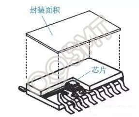
To evaluate the quality of integrated circuit packaging technology, an important indicator is the packaging ratio:
Package ratio = chip area/package area
The closer this ratio is to 1, the better. In the integrated circuit packaging schematic shown in Figure 1, the chip area is generally very small, and the packaging area is limited by the pin spacing, making it difficult to further reduce it.
Figure 1 Schematic diagram of integrated circuit packaging
The packaging technology of integrated circuits has gone through several generations of changes, from DIP, QFP, PGA, BGA to CSP and then to MCM. The packaging ratio of the chip is getting closer and closer to 1, the number of pins has increased, the pin spacing has decreased, and the weight of the chip has been reduced. , power consumption is reduced, and huge progress has been made in technical indicators, operating frequency, temperature resistance, reliability and applicability.
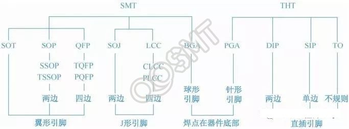
Figure 2 shows a summary of commonly used semiconductor device packaging forms and characteristics.
Figure 2 Package forms and characteristics of commonly used semiconductor devices
2. Packaging form of SMT integrated circuits
1.SO package
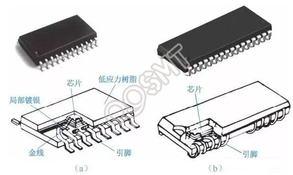
Small-scale integrated circuits with relatively few leads mostly use this small package, as shown in Figure 2-28. SO packages are divided into several types. Those with a chip width less than 0.15 in and a relatively small number of electrode pins (generally between 8 and 40 pins) are called SOP packages; those with a width above 0.25 in and a number of electrode pins above 44 , called SOL package, this kind of chip is commonly found in random access memory (RAM). Chips with a width of more than 0.6 inches and a number of electrode pins of more than 44 are called SOW packages. This type of chip is commonly found in programmable memories (E2PROM). Some SOP packages adopt miniaturized or thin packages, which are called SSOP packages and TSOP packages respectively. The pins of most SO packages use wing-shaped electrodes, and some memories use J-shaped electrodes (called SOJ), which is beneficial to expanding the storage capacity on the socket. Figure 3 (a) and (b), respectively, have wing-shaped leads. SOP package structure with pins and "J" shaped pins. The pin pitches of SO packages are 1.27 mm, 1.0 mm, 0.8 mm, 0.65 mm and 0.5 mm.
Figure 3 Wing-shaped lead and “J”-shaped lead packaging structure of SOP
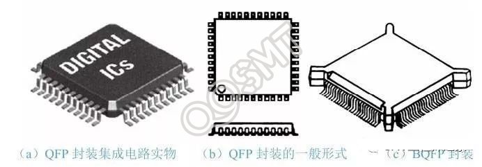
2.QFP packaging
QFP (Quad Flat Pockage) is a four-side flat package. It is one of the main packaging forms of SMT integrated circuits. The pins are drawn out from the four sides in a wing (L) shape. There are three types of base materials: ceramic, metal and plastic. In terms of quantity, plastic packaging accounts for the vast majority. When the material is not specifically indicated, in most cases it is plastic QFP. Plastic QFP is the most popular multi-pin LSI package. Not only used in digital logic LSI circuits such as microprocessors and gate arrays, but also in analog LSI circuits such as VTR signal processing and audio signal processing. The pin center distance is available in various specifications such as 1.0 mm, 0.8 mm, 0.65 mm, 0.5 mm, 0.4 mm, 0.3 mm, etc. The minimum limit of the pin spacing is 0.3 mm and the maximum is 1.27 mm. The maximum number of pins in the 0.65 mm center pitch specification is 304.
To prevent pin deformation, several improved QFP varieties have emerged. For example, BQFP has resin buffer pads (lugs) at the four corners of the package. It sets protrusions at the four corners of the package body to prevent the leads from bending and deforming during transportation or operation. Figure 4 is the appearance of a QFP package integrated circuit.
Figure 4 Common QFP packaged integrated circuits
3.PLCC packaging
PLCC is a pinned plastic chip carrier package of an integrated circuit. Its pins are hooked inwards, called hook-shaped (J-shaped) electrodes. The number of electrode pins is 16 to 84, and the spacing is 1.27 mm. Its appearance and packaging The structure is shown in Figure 5. Most of the integrated circuits packaged by PLCC are programmable memories. The chip can be installed on a special socket and can be easily removed to rewrite the data in it; in order to reduce the cost of the socket, the PLCC chip can also be directly welded on the circuit board, but manual welding is more difficult.
Figure 5 PLCC packaging structure
PLCC has two shapes: square and rectangular. The number of rectangular leads is 18, 22, 28, and 32 respectively; the number of square leads is 16, 20, 24, 28, 44, 52, 68, 84, 100, 124, and 156 . PLCC occupies a small coverage area, has high lead strength, is not easily deformed, and has good coplanarity.
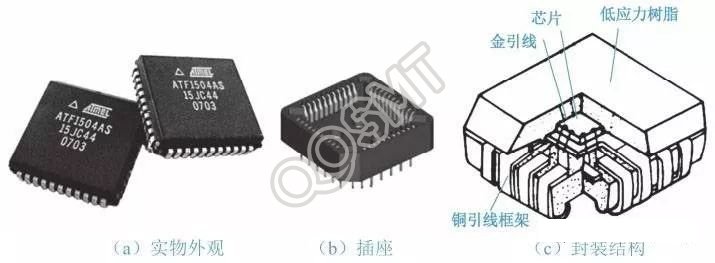
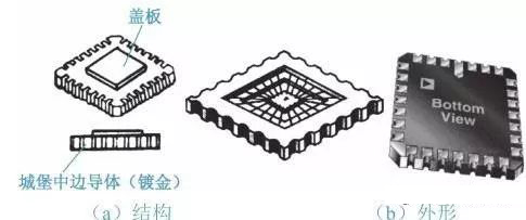
4.LCCC package
LCCC is a package without pins in a chip integrated circuit packaged on a ceramic chip carrier; the chip is packaged on the ceramic carrier, with two shapes: square and rectangular, with leadless electrode soldering terminals arranged on the four sides of the bottom surface of the package. The number of electrodes is 16, 20, 24, 28, 44, 52, 68, 84, 100, 124 and 156 for squares and 18, 22, 28 and 32 for rectangles respectively. There are two types of pin spacing: 1.0 mm and 1.27 mm. Its structure and appearance are shown in Figure 6.
Figure 6 LCCC packaged integrated circuit
The characteristic of the LCCC lead-out terminal is that there is a castle-shaped metallized groove on the side of the ceramic shell connected to the gold-plated electrode on the bottom of the shell, which provides a short signal path, low inductance and capacitance losses, and can be used in high-frequency working conditions, such as micro Processor units, gate arrays and memories.
The chip of the LCCC integrated circuit is fully sealed and has high reliability but high price. It is mainly used in military products, and the issue of whether the thermal expansion coefficient between the device and the circuit board is consistent must be considered.
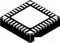
5.PQFN packaging
PQFN is a leadless package, square or rectangular in shape, with a large exposed pad in the center of the bottom of the package to improve heat dissipation. There are conductive pads on the periphery of the package surrounding the large pad that make the electrical connection. Because the PQFN package does not have wing-shaped pins like SOP, QFP, etc., the conductive path between the internal pins and the pad is short, the self-inductance coefficient and the wiring resistance within the package are very low, so it can provide good electrical performance. Its appearance is shown in Figure 7.
Figure 7 Quad Flat No-Lead Plastic Package (PQFN)
PQFNs have become ideal for many new applications due to their good electrical and thermal properties, small size, and light weight. PQFN is very suitable for use in high-density products such as mobile phones, digital cameras, PDAs, DVs, smart cards and other portable electronic devices.
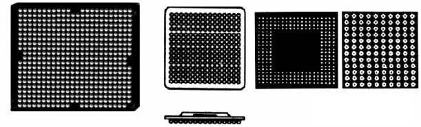
6.BGA package
BGA packaging, also known as ball grid array packaging, changes the J-shaped or wing-shaped electrode pins of the original device PLCC/QFP package into spherical pins; the electrodes sequentially drawn out from the "single linear" around the device body become the bottom surface of the body. Below is a "full plane" grid array arrangement. In this way, the pin spacing can be dispersed and the number of pins can be increased. The solder ball array can be fully or partially distributed on the bottom surface of the device, as shown in Figure 8.
Figure 8 BGA packaged integrated circuit
(1) The BGA method can significantly reduce the chip packaging surface area: Assume that a large-scale integrated circuit has 400 I/O electrode pins, and the pin spacing is also taken to be 1.27 mm, then a square QFP chip has 100 pins on each side , the side length is at least 127 mm, and the surface area of the chip must be more than 160 cm2; while the electrode pins of the square BGA chip are evenly arranged under the chip in 20×20 rows, the side length is only 25.4 mm, and the surface area of the chip is not even to 7 cm2. It can be seen that for large-scale integrated circuits with the same functions, the size of the BGA package is much smaller than that of QFP, which is conducive to increasing the density of assembly on the PCB circuit board.
(2) From the perspective of assembly and welding, the mounting tolerance of BGA chips is 0.3 mm, which is much lower than the mounting accuracy requirement of 0.08 mm for QFP chips. This significantly improves the mounting reliability of BGA chips and significantly reduces the process error rate. Ordinary multi-functional placement machines and reflow soldering equipment can basically meet the assembly requirements.
(3) The use of BGA chips shortens the average line length of the product and improves the frequency response and other electrical properties of the circuit.
(4) When soldering with reflow soldering equipment, the high surface tension of the solder ball causes the self-calibration effect of the chip (also known as the "self-centering" or "self-positioning" effect), which improves the quality of assembly welding.
Precisely because BGA packaging has obvious advantages, the BGA varieties of large-scale integrated circuits are also rapidly diversifying. Now there are many forms, such as ceramic BGA (CBGA), plastic BGA (PBGA) and micro BGA (Micro-BGA, μBGA or CSP). The main difference between the first two is the base material of the package. For example, CBGA uses ceramic. PBGA uses BT resin; the latter refers to those micro integrated circuits whose package size is close to the chip size.
Currently, the general BGA chips that can be seen have three types of solder ball spacing: 1.5 mm, 1.27 mm, and 1.0 mm; while the μBGA chips have a variety of solder ball spacings of 0.8 mm, 0.65 mm, 0.5 mm, 0.4 mm, and 0.3 mm.
7.CSP packaging
The full name of CSP is Chip Sceie package, which means chip size package. It is the product of further miniaturization of BGA. The size of the bare chip is the same as the package size. That is, the side length of the packaged IC is no more than 1.2 times that of the chip, and the IC area is only no more than 1.4 times larger than the die. CSP packaging can make the ratio of chip area to package area exceed 1:1.14, which is very close to the ideal situation of 1:1.
Under the same chip area, the number of pins that CSP can achieve is obviously much higher than that of TSOP and BGA. TSOP has a maximum of 304 pins, BGA’s pin limit can reach 600, and CSP can theoretically reach 1,000 pins. Due to such highly integrated features, the distance from the chip to the pin is greatly shortened, the impedance of the line is significantly reduced, and the attenuation and interference of the signal are greatly reduced. The CSP package is also very thin, and the most effective heat dissipation path from the metal substrate to the heat sink is only 0.2 mm, which improves the chip's heat dissipation capability.
The current CSP is also mainly used for packaging of integrated circuits with a small number of I/O terminals, such as computer memory sticks and portable electronic products. In the future, it will be widely used in emerging products such as information appliances (IA), digital televisions (DTV), e-books (E-Books), wireless networks WLAN/GigabitEthemet, and ADSL/.