How to accurately mount 0201 components
Jan 21, 2024
In order to maintain the coherence of the production system, the nozzle must be able to move in all three directions, i.e. along the X, Y and Z axes - this is important because on all production machines there is no control of the Y axis. However, in order to maintain placement accuracy within tolerances, Y-direction control is necessary to center the component on the nozzle (Figure 1). Naturally, this alignment has tighter tolerances for 0201 than for other parts.ed-loop real-time feedback on all three axes, the need for feeder calibration is virtually eliminated. Without real-time closed-loop feedback on all three axes, feeder calibration is critical.
This article explains that smaller components and narrower pitches pose new challenges for circuit board assembly. Understanding these placement issues can get products to market faster and with fewer defects.
The reality facing the industry is that parts are getting smaller and smaller. For example, 0201 chip capacitors are 75% smaller than 0402 and take up 66% less area on the circuit board. These components will appear on some general-purpose printed circuit boards early this decade, and the even smaller 01005 chip By 2005, these components will be seen on modular circuit boards where space is at a premium.
Because board space is so precious for many new products, smaller components will be used even more widely, even though they cost more. This new miniaturization requires increased placement accuracy without reducing speed.
Identify the challenges faced
Small components pose many problems. Higher density - the main reason that plagues smaller components - makes the placement task an order of magnitude more difficult. For example, 0201 components often require smaller pad sizes to prevent solder smears and allow for solderless soldering. Also, smaller pads mean narrower component spacing. While these allow designers to achieve the higher density required for highly functional and compact products, they also complicate the situation. For high-density PCBs, placement accuracy directly affects the number of assembly defects after reflow soldering. For example, placement offset increases the chances of tin bridges, tin beads, component erection, and component misalignment pads.
So, what do we need? Today, a realistic production goal is to achieve 99.9% pick-up rate with a 3σ placement accuracy of ±60µm. To achieve this goal, machine accuracy becomes a primary issue.
For example, Motorola’s tests show that changes as small as 0.025mm in placement offset can significantly affect defect levels. For standard pads (tested with 100,000 components), the impact of placement offset of y<0.075mm, x<0.075mm on defects is similar to that of no offset. However, when the offset increases to <0.1mm, the defect level rises to over 5000ppm. While this absolute distance means small, research shows the process leaves little room for error. Also, the placement operation involves more than itself. It includes pick-up reliability, accurate component visual identification and placement repeatability. In fact, tests have shown that 0201 components require 99% pick-up reliability.
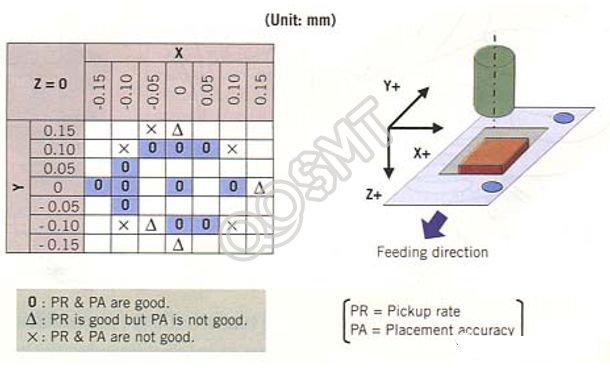
Pickup position tolerance
In order to maintain the coherence of the production system, the nozzle must be able to move in all three directions, i.e. along the X, Y and Z axes - this is important because on all production machines there is no control of the Y axis. However, in order to maintain placement accuracy within tolerances, Y-direction control is necessary to center the component on the nozzle (Figure 1). Naturally, this alignment has tighter tolerances for 0201 than for other parts.ed-loop real-time feedback on all three axes, the need for feeder calibration is virtually eliminated. Without real-time closed-loop feedback on all three axes, feeder calibration is critical.
Research shows that an accuracy of ±0.07mm in the Y direction is necessary to ensure successful 0201 placement. Also, successful placement requires tolerances of ±0.1mm in the X direction and ±0.1mm in the Z direction to achieve the 0.2mm target. Correcting the X/Y axis movement of the nozzle is key to ensuring stable and consistent component pickup.
Movement on solder paste
Another mounting issue is that under certain conditions, 0201 will not stay in its mounted position. Consider a situation where a 0201 capacitor is mounted on a PCB printed with solder paste and flux, hoping to obtain a controlled travel of ±0.05mm and a component spacing of 0.15mm. Tests have shown that for a placement accuracy of 3σ in the Y direction, components with an overtravel of less than 0.05mm on the board will sometimes slide more than 60µm in the short side direction.
What will happen? Interestingly, further investigation revealed that component slippage due to overtravel did not occur when the component was simply mounted on flux, but it did occur when mounted on solder paste. Conclusion: The problem is the particle diameter of the solder paste. To compensate for Z-axis correction, the machine must have a real-time feedback mechanism that measures the thickness of each component.
When the particle size is larger than 20µm, component deflection is possible because the particles are unevenly distributed on the pad. Because component placement times are milliseconds, any uneven surface may cause part deflection or movement. This is why hot air solder leveling (HASL) boards are not suitable for 0201 placement, in contrast to 0402 approved HASL.
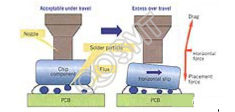
Figure 2. When the component overtravels and impacts the solder particles, the reaction force changes the axial direction of the suction nozzle and generates a horizontal force, causing the component to deflect.
Therefore, overtravel reduces placement accuracy. It may also increase solder bridging in high-density mounting because components can push solder paste out from under the part when using solderless pads (Figure 2). Therefore, overtravel can be defined as making the gap between the component and the PCB smaller than the solder particle size, that is, the placement system must control the gap to maintain it at 40-60µm. One factor that comes into play is the support of the board, without supporting components there is the possibility of being dropped from an excessive height or being forced into the solder paste. To accurately control travel, the board's support system must provide adequate correction for the board's camber.
improvements needed
To achieve effective use of 0201 components, part of the solution will be found in the design improvement of the nozzle. Because the components are so small, they require a nozzle design that maximizes the contact surface area for the vacuum while providing a form factor that does not interfere with high-density layouts. In addition, the nozzle must be highly wear-resistant, as its corrosive effects are exacerbated by the small contact area. All of these must be aware of how to meet and deal with the upcoming challenges of 01005 components.
The current results provide a 0.75 cycle time, 60µm (3σ) accuracy, and 99.9% pick-up rate for a 0.25mm gap. The goal was to achieve a cycle time of 0.075 seconds per part, an accuracy of 40µm (3σ), and a pickup rate of 99.9% for a 0.10-0.15mm gap. A specially developed tape feeder for 0201 components should also facilitate more precise and faster component placement.
in conclusion
A real economic issue is that boards produced with 0201 components will be more expensive than their larger counterparts. Additionally, tighter tolerances necessarily require increased process control, more thorough preventive maintenance, more training and process knowledge, and increased awareness of scrap and inspection/repair activities.
Preventative maintenance has always been an important part of production, but now it’s even more important due to 0201 placement. Because tolerances and accessibility of errors are as small as the components themselves, preventive maintenance is a more important manufacturing cost factor for the 0201 line than for other components. Similarly, it appears that use of 0201 will require more frequent nozzle cleaning, camera cleaning, and machine placement measurements and adjustments. The height at which components are picked up and placed will be critical. For initial component pick-up, feeder axis adjustment is required, although the machine can compensate for component offset in the pick-up position.