SMT (surface assembly) core process analysis, basic process flow and process design explanation
Jan 21, 2024
1.Reflow soldering process
2. Wave soldering process
The welding of surface-mounted printed circuit board assembly (PCBA) mainly includes two processes: reflow soldering and wave soldering, which constitute the basic process flow of SMT assembly.
1.Reflow soldering process
Reflow soldering refers to a soldering process that realizes the mechanical and electrical connection between the solder terminals or pins of surface-mounted components and the PCB pads by melting the solder paste pre-printed on the PCB pads.
1) Process characteristics
(1) The application of solder (in the form of solder paste) and heating are performed separately, and the size of the solder joints is controllable;
(2) The solder paste is distributed by printing, and each soldering surface generally uses only one steel mesh for solder paste printing;
(3) The main function of the reflow soldering furnace is to heat the solder paste. It heats the PCBA as a whole placed in the furnace. During the second soldering, the solder joints soldered for the first time will be re-melted.
2) Process flow
Print solder paste→SMT→Reflow soldering, as shown in Figure 1-3.
Figure 1-3 Reflow soldering process flow
2. Wave soldering process
Wave soldering refers to spraying molten solder (tin-containing solder) into a solder wave through a mechanical pump or electromagnetic pump, so that the PCB pre-installed with components can pass through the solder wave to realize the soldering ends or pins of the components. A soldering process for mechanical and electrical connections to PCB jacks/pads.
1) Process characteristics
(1) Apply solder and heat to the PCB.
(2) The application of heat is mainly conducted through the molten solder. The amount of heat applied to the PCB mainly depends on the temperature of the molten solder and the contact time between the molten solder and the PCB (soldering time).
(3) The size and fillability of solder joints mainly depend on the design of the pad and the installation gap between the hole and the lead. In other words, the size of the wave soldering joint mainly depends on the design.
(4) When welding SMD, there is a "shielding effect" and soldering leakage is prone to occur. The so-called "shadowing effect" refers to the phenomenon that the chip SMD package blocks the solder wave from contacting the pad/solder terminal.
2) Process flow
Dispensing→SMT→Curing→Wave soldering, as shown in Figure 1-4.
Figure 1-4 Wave soldering process flow
PCBA assembly process design
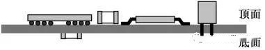
1. The PCBA assembly process design determines the layout of the components on the front and back of the PCBA. The main layout design is shown in Figures 1-5 to 1-9.
Figure 1-5 Double-sided SMD layout design
Figure 1-9 Layout design for selective wave soldering using moving nozzles on the bottom surface
1. Full SMD layout design
With the development of component packaging technology, basically all types of components can be packaged by surface assembly. Therefore, using full SMD design as much as possible will help simplify the process and increase assembly density.
Depending on the number of components and design requirements, it can be designed as a single-sided full SMD or double-sided full SMD layout (see Figure 1-5). For a double-sided full SMD layout, the components laid out on the bottom surface should meet the most basic requirement of not falling off during soldering on the top surface.
The assembly process is as follows.
(1) Bottom surface: Print solder paste → SMT → Reflow soldering.
(2) Top surface: Print solder paste → SMT → Reflow soldering.
The reason why the bottom surface is welded first is because the SMD laid out on the bottom generally takes into account the welding requirements that it cannot fall off.
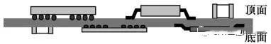
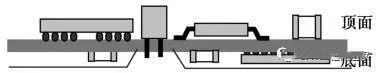
2. Top surface mixed installation, bottom surface SMD layout design
This is a common layout form at present. According to the welding method of plug-in components, it can be subdivided into three types of layouts, namely wave soldering, pallet selective wave soldering and moving nozzle selective wave soldering or manual welding. Due to different welding processes, the design requirements are slightly different.
1) The bottom surface adopts wave soldering layout design
The layout design using wave soldering on the bottom surface is shown in Figure 1-6. This type of layout is suitable for situations where complex surface assembly components (SMDs not suitable for wave soldering) can be laid out on one side.
Figure 1-6 Layout design using wave soldering on the bottom surface
The bottom surface can generally only be packaged with wave soldering, such as chip components in the range of 0603 to 1206, SOP with lead spacing greater than or equal to 1mm, etc.
For wave soldering layout design, the SMD on it must be fixed by dispensing glue first. The assembly process used is as follows:
(1) Top surface: Print solder paste → SMT → Reflow soldering.
(2) Bottom surface: dispensing → patch → curing.
(3) Top surface: plug-in.
(4) Bottom surface: wave soldering.
The reason why the top surface is soldered first is because, on the one hand, the bare PCB is relatively flat before welding; on the other hand, because the curing temperature of the bottom glue is relatively low (≤150°C), it will not cause damage to the components that have been soldered on the top surface. adverse effects.
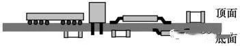
2) The bottom surface adopts the layout design of pallet selective wave soldering
The layout design using tray selective wave soldering on the bottom surface is shown in Figure 1-7. This type of layout is suitable for situations where there are a large number of SMDs, the layout cannot fit on one side, and there are many plug-in components.
Figure 1-7 Layout design using pallet selective wave soldering on the bottom surface
There are many requirements for the bottom layout. First, the SMD components cannot be too high; second, the distance between the wave soldering components and the SMD protected by the tray must meet the design requirements of tooling and temperature.
The layout design of pallet selective wave soldering and its assembly process are as follows:
(1) Bottom surface: Print solder paste → SMT → Reflow soldering.
(2) Top surface: Print solder paste → SMT → Reflow soldering.
(3) Top surface: plug-in.
(4) Bottom surface: Add pallet wave soldering, as shown in Figure 1-8.
Figure 1-8 Pallet
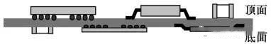
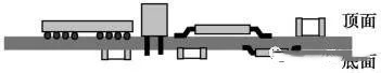
3) The bottom surface adopts the layout design of selective wave soldering with moving nozzles
The bottom surface adopts the layout design of selective wave soldering with moving nozzles. This type of layout is suitable for situations where there are a large number of SMDs, the layout is not limited to one side, and there are only a few plug-in components.
The bottom layout is basically the same as the double-sided full SMD, as long as the distance between the insertion pins and surrounding components meets the nozzle welding requirements.
The bottom surface adopts the layout design of selective wave soldering with moving nozzles. The assembly process is as follows:
(1) Bottom surface: Print solder paste → SMT → Reflow soldering.
(2) Top surface: Print solder paste → SMT → Reflow soldering.
(3) Bottom surface: selective wave soldering with moving nozzle.