SMT solder joint welding reliability
Jan 21, 2024
According to the understanding of the book written by expert Jia Zhongzhong, the reliability of SMT solder joint welding is mainly determined by SMT welding process factors to achieve good surface wetting and then form IMC. The quality of IMC directly determines the reliability of the solder joint, so we will introduce it to you in detail. SMT welding process elements, understanding of surface wetting and solderability, introduction to IMC (metal compounds), introduction to black disk, welding quality judgment, basic concepts of reliability, etc.
1. SMT welding process elements
The occurrence of PCBA welding defects is largely related to solder paste printing, stencil design, pad design and temperature curve settings, and is related to process. The SMT process, according to business division, can generally be divided into process design, process trial production and process control, as shown in Figure 1. Its core goal is to reduce soldering, bridging, and Less tin and shift, resulting in the expected solder joint quality.
In every business, there is a set of process control points, among which pad design, stencil design, solder paste printing and PCB support are the key points of process control.
As the size of component pads and intervals continues to shrink, the area ratio of the stencil window and the gap between the stencil and PCB printing are becoming more and more important. The former is related to the transfer rate of solder paste, while the latter is related to the consistency of solder paste printing volume and the good rate of printing. In order to obtain a solder paste transfer rate of more than 75%, based on experience, it is generally required that the area ratio of the stencil window to the side wall is greater than or equal to 0.66; to obtain a stable amount of solder paste that meets design expectations, the ratio between the stencil and the PCB during printing must be The smaller the gap, the better. It is not a difficult task to achieve an area ratio greater than or equal to 0.66, but it is a very difficult task to eliminate the gap between the stencil and the PCB. This is because the gap between the stencil and the PCB is closely related to the design of the PCB and the warpage of the PCB. , PCB support during printing, etc. are related to many factors. Sometimes, the product design and equipment used are uncontrollable, and this is precisely the key to the assembly of fine-pitch components! Poor welding of CSP with 0.4mm pin pitch, multi-row pin QFN, LGA, and SGA is almost 100% related to this. Therefore, in advanced professional foundries, many very effective PCB support toolings have been invented to correct the fin curvature of PCBs to ensure zero-gap printing.
2. Understanding of surface wetting and solderability:
1. Surface wetting
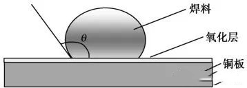
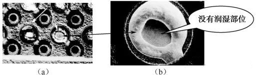
Surface wetting refers to the phenomenon that molten solder spreads and covers the surface of the metal to be welded during welding. Wetting indicates that dissolution and diffusion occur between the liquid solder and the surface to be soldered, forming an intermetallic compound (IMC), which is a sign of good soldering. When we immerse a solid metal piece into a liquid solder bath, there is contact between the metal piece and the liquid solder, but this does not mean that the metal piece has been wetted by the liquid solder, because there may be a barrier layer between them, only You can see if it's wet by pulling the small piece of metal out of the solder bath. Wetting can only occur when the liquid solder is in close contact with the metal surface to be soldered, and sufficient attraction can only be guaranteed at that time. If there are any firmly attached contaminants on the surface to be welded, such as an oxide film, it will act as a barrier to the metal's connection and prevent wetting. On a contaminated surface, a drop of solder behaves the same as a drop of water on a greased plate, as shown in Figure 2. It cannot spread and the contact angle θ is greater than 90°.
Figure 1-31 Solder droplets on oxidized plates cannot wet
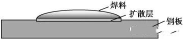
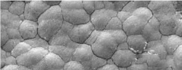
If the surface to be soldered is clean, then the position of their metal atoms is close to the interface, so wetting occurs and the solder will spread on the contact surface, as shown in Figure 2. At this time, the solder and matrix atoms are very close, thus forming an alloy at the interface that attracts each other, ensuring good electrical contact and adhesion.
Figure 1-32 Solder droplets on the clean plate wet and grow a diffusion layer at the interface
2.Weldability
Weldability refers to the ability of the base metal to be welded to be welded under specified time and temperature. It is related to the heat capacity, heating temperature and surface cleanliness of the base material (component or PCB pad) being welded. Weldability is usually evaluated by the dipping method or the wetting balance method. These two methods are essentially the same, which is to see whether the base metal to be welded can be wetted under the specified time and temperature. Therefore, it can be said that solderability and wettability are closely related. In the immersion test, one or more of the following phenomena can be observed on the surface of the sample taken out of the molten solder tank.
(1) Non-wetting: The surface becomes uncovered again, without any visible interaction with the solder, and the soldered surface maintains its original color. If the oxide film on the surface to be welded is too thick and cannot be removed by the flux within the effective welding time, non-wetting will occur.
(2) Wetting: After the molten solder is removed, a thin layer of solder still remains on the welded surface, proving that intermetallic interaction has occurred. Complete wetting means leaving a uniform, smooth, crack-free, and well-adhered layer of solder on the surface of the metal being welded.
(3) Partial wetting: Some parts of the welded surface are wetted, and some parts are not wetted. (4) Weak wetting: The surface is wetted at first, but then the solder shrinks from part of the surface into droplets, leaving a thin layer of solder in the weakly wetted area.
3. Intermetallic compounds (IMC)
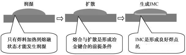
The formation process of solder joints
The formation process of solder joints can be divided into three stages: solder wetting (spreading), base metal fusion/diffusion, and intermetallic compound (IMC) formation, as shown in Figure 3.
Figure 3 Welding process
Intermetallic compounds (IMC)
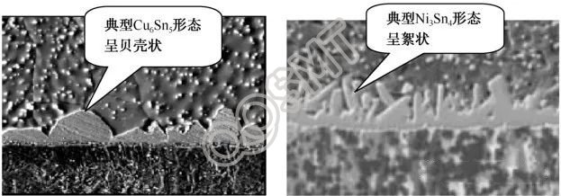
Intermetallic compound, the full name in English is Intermetallic Compound, abbreviated as IMC. It is the product of interface reaction and is also a sign of good solder joints. Among various solder alloys, a large amount of Sn is the protagonist, and it is the main element involved in the formation of IMC. The remaining elements only play a supporting role, mainly to lower the melting point of the solder and suppress the growth of IMC. A small amount of Cu and Ni will also affect the structure of IMC. Under lead process conditions, the typical morphology of IMC formed at the interface between tin-lead solder and Cu and Ni is shown in Figure 4. Only Sn in the solder participates in the formation of IMC, and the composition of IMC is fixed.
Figure 4 Morphology of Cu6Sn5 and Ni3Sn4
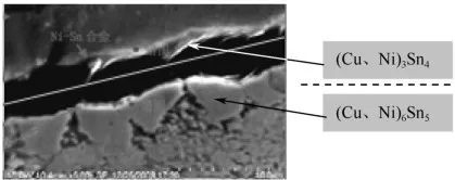
Under lead-free process conditions, due to the wide variety of lead-free solders used, the composition and form of IMC are relatively complex. For example, when using SAC305 solder, the IMC formed at the interface between the solder and the Ni base is a double-layer ternary alloy layer of (Cu, Ni) 6Sn5 and (Cu, Ni) 3Sn4, as shown in Figure 5. This is different from lead soldering.
Figure 5 Morphology of (Cu, Ni) 6Sn5 and (Cu, Ni) 3Sn4
The formation and development of IMC
It is generally believed that a very thick IMC is a defect. Because IMC is relatively brittle, the thermal expansion coefficient is very different from the base material (electrodes, components or substrates during packaging). If IMC grows very thick, cracks will easily occur. Therefore, mastering the formation and growth mechanism of the interface reaction layer is very important to ensure the reliability of solder joints!
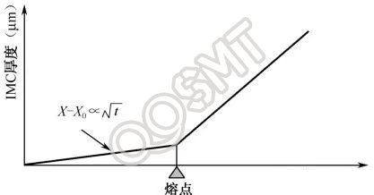
The formation and development of IMC are related to the solder alloy, base metal type, soldering temperature and time, and the flow state of the solder. Generally speaking, at temperatures below the melting point of solder, the formation of IMC proceeds by diffusion, and the speed is very slow, and its thickness is proportional to the square root of time; at temperatures above the melting point of solder, the formation of IMC proceeds by reaction, and the higher the temperature, the longer the time. The longer it is, the thicker it is, as shown in Figure 6. Therefore, too high temperature and too long liquid time will lead to excessively thick IMC.
Figure 6 The relationship between IMC growth thickness and temperature
Under lead process conditions, due to the inhibitory effect of Pb, the IMC formed by Cu and SnPb solder generally does not exceed 2.5μm. However, under lead-free process conditions, since the solubility of Cu in molten SAC305 is 8.6 times higher than that in Sn63/Pb37, a thicker IMC layer will be formed when reacting with SAC, which is not conducive to the Lead solder joint reliability.
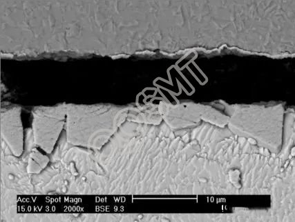
There is another phenomenon worthy of further study, that is, when Cu and SAC305 are reflowed for the first time (including the BGA ball mounting process), the IMC formed is relatively thick (≥10μm). If the IMC is reflowed again, it may form an ultra-wide, discontinuous The block IMC is shown in Figure 7. This is an IMC structure with relatively low tensile strength. If it appears on BGA solder joints, it may cause hidden dangers in reliability.
Figure 7 Ultra-wide, discontinuous block IMC
Fracture failure related to interfacial diffusion
1) Gold brittle failure
If the Au is too thick (for electroplating Ni/Au, it should generally be less than 0.08μm), during use, the Au dispersed in the solder will diffuse near the Ni/Sn interface to form a strip of (Ni-Au) Sn4 intermetallic compounds. The enrichment of this IMC at the interface often leads to brittle failure.
2) Interface coupling phenomenon
The reaction on the PCB pad interface is not only related to this interface, but also to the device pin material and coating. For example, when the pad is made of Ni/Au and the device lead is made of Cu alloy, Cu will often diffuse to the Ni/Sn interface, causing the interface to form (Cu, Ni) 3Sn4-(Cu, Ni) 6Sn5, which will lead to large-scale solder joints. Invalid.
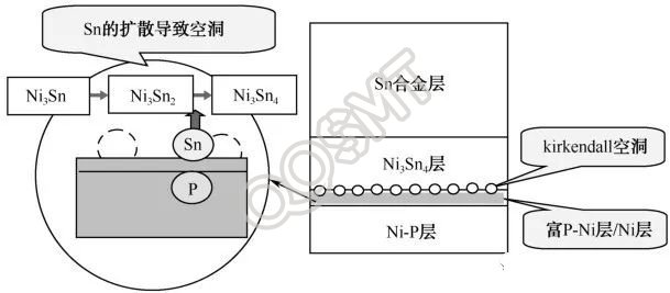
3)kirkendall hollow
ENIG coatings are prone to the famous kirkendall voids, as shown in Figure 8.
Figure 8 Kirkendall void phenomenon
Kirkendall voids are related to high temperature aging time. The longer the time, the more voids there are. If exposed to 125°C, continuous cracks will form in 40 days.
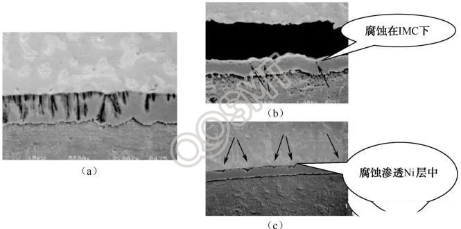
3. Black disk
"Black disk" was first proposed by Puttlitz in 1990.
1) Definition
Because the solder joint fracture surface is gray and black, it is called a black disk, as shown in Figure 9. Fractures related to the black disk all occur under the IMC of the Sn-Ni interface. The darker the pad color, the thinner the IMC, from black to black gray!
Figure 9 "Black plate" color
2) Three typical characteristics related to black disks
a. Corrosion cracks (mud cracks) can be observed on the fracture surface (under IMC), as shown in Figure 10. The more cracks there are, the lower the connection strength of the solder joints (the cracks are completely non-wetting), and the harder it is to form IMC. Because lead-free solder joints are relatively hard and are directly transmitted to the interface after being stressed, lead-free solder joints are more likely to fail due to black disks.
Figure 10 Mud crack characteristics of “Black Pan”
b. From the polished cross section, it can be observed that "corrosion" has penetrated and even penetrated the Ni layer into the Cu matrix, commonly known as the "gold thorn" feature, as shown in Figure 11.
Figure 11 The "golden thorn" characteristics of the "black plate"
c. The P content near the Ni surface is relatively high (up to about 20%, twice the normal level), but it should be pointed out that rich phosphorus is not the direct cause of solder joint failure.
4. Identification of solder joint quality
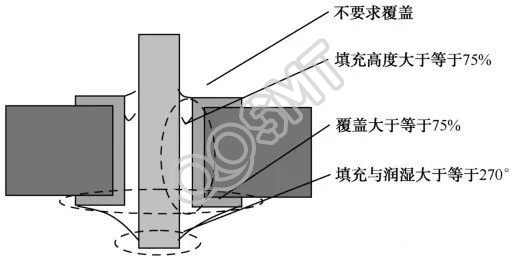
1. Judgment of solder joint quality of plug-in components
Appearance inspection is generally carried out in accordance with the requirements of IPC-A-610G. Since there are many types of solder joints, it is difficult to describe them simply. Therefore, IPC decomposes the solder joints into multiple dimensions and evaluates them with a single requirement. This is a way to deal with complex problems and is worth learning. The qualification requirements for solder joints of plug-in components are shown in Figure 12
2. Judgment of solder joint quality of SMT components: There is a lot of information in this part. You can consult this standard document according to your needs. I will not explain it in detail here!
5. Basic concepts of solder joint reliability and failure analysis
basic concept
1) Reliability Reliability refers to the ability of a product (here, solder joints) to complete specified functions under given conditions and within a specified time. It is a probability relative to certain load conditions, so reliability must refer to reliability under certain load conditions. The load conditions of different electronic products will be different. For example, automotive electronic systems are subject to periodic loads and vibration loads caused by hot and cold environments. Thermal cycle testing is to simulate this thermo-mechanical load to analyze the cause of solder joint failure. A load condition refers to any condition imposed on a system that deteriorates its performance or affects its reliability. Load is a generalized load, such as thermal shock, thermal cycle, temperature, humidity, voltage, current, mechanical vibration, etc.
2) Failure (Failure) Failure, loss of function or reduction to the point that it cannot meet specified requirements.
3) Failure Mode (Failure Mode) Failure mode, the manifestation of failure phenomenon, has nothing to do with the cause, such as open circuit, short circuit, parameter drift, instability, etc.
4) Failure Mechanism Failure mechanism is the process of product failure due to physical, chemical, mechanical and other reasons, such as creep-stress release fracture, tensile fracture, crack propagation fracture, Electromigration short circuit is sometimes described as a failure mechanism in engineering. The reason why failure modes and failure mechanisms are distinguished is that sometimes the same failure mode is not necessarily caused by the same failure mechanism. On the contrary, the same failure mechanism has different failure modes in the form of failure. For example, "electromigration", which represents a semiconductor circuit failure, can cause various failure modes such as short circuit, open circuit, and deterioration of characteristics depending on the form in which it occurs.
5) Accelerated test Accelerated test is a rapid test method. It does this by using a test environment that is more severe than what the device (in this case, the solder joint) is subjected to in normal use. Because of the higher stresses used, care must be taken when conducting accelerated testing not to introduce failure modes that would not occur in normal use. There are two main categories of accelerated testing, each with a clear purpose:
(1) Accelerated life test - estimated life;
(2) Accelerated stress testing - identify (or confirm) and correct weak links.
Commonly used accelerated tests include:
(1) Periodic stress tests with fixed cycles (such as thermal cycle tests, hot shockhit test);
(2) Step stress spectrum test;
(3) Progressive stress spectrum test;
(4) Highly accelerated life test (HALT) (equipment level);
(5) Highly accelerated stress screening (HASS) (equipment level);
(6) Highly accelerated temperature and humidity stress test (HAST) (part level). Note that the Environmental Stress Screening (ESS) test used in the production of high-reliability electronic products is not an accelerated test. It is a screening method to eliminate defective solder joints.