You must know the SMT PCB visual inspection specifications-golden fingers and PCB surface treatment
Jan 21, 2024
2. Surface treatment OSP(ENTEK) PCB board/Immersion Silver/LF
Foreword: As a main component of SMT, the importance of the PCB board is undoubted, so the incoming material inspection of the PCB board is also very important. The quality of the PCB board is crucial to the entire SMT assembly, so we will work with you in the near future. Discuss some key items in PCB inspection. This issue discusses the surface treatment of PCB gold fingers and holes!
1. PCB Gold Finger inspection specifications
1. Gold finger gold plating thickness
1) Nickel plating thickness:≧ 100 u".
2) Gold plating thickness: Made according to actual production specifications.
3) Gold finger Pad size: ± 2mil
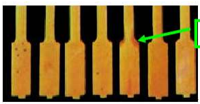
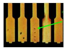
2. No protrusions or gaps are allowed between gold fingers.
3. Gold fingers are not allowed to discolor.
4. The gold finger should not be scratched to expose the copper layer and substrate, nor should it be exposed to the nickel plating. The scratched part should not exceed 1/5 of the total number of pins.
5. Gold fingers are not allowed to have tin, paint, residual glue or other contaminants.
6. Gold fingers do not allow protrusions or surface plating on the surface.
7. The gold fingers are not allowed to have pressure dents or wrinkles, and there must be no burrs of copper chips or warping of the gold fingers after molding.
8. The gold finger is allowed to test pin points, but the substrate (copper or nickel) is not allowed to be exposed for testing. Rough plating is also not allowed. The number of plating needle points (Pit) cannot exceed 5 points, but the commonality of the gold finger is not allowed. There are electroplated pin points.
9. Depressions (dots) The depressions (dots) of the gold finger must not expose the base material (copper or nickel). The maximum diameter of depressions (spots) cannot exceed 10 mil and there cannot be more than two spots on a single surface.
10. There should be no copper shavings left at the end of the gold finger. 3.6.11 3.6.11 Adhesion test: ﹙adhesion test﹚Use 3M SCOTCH NO.600 wide tape with a width of 0.5" and stick it on the solder mask with a close length of about 2". After 30 seconds, straighten it in the 90-degree direction. When pulling it up, there should be no plating peeling off or warping. If there is any phenomenon, it will be regarded as a serious defect.
2. Surface treatment OSP(ENTEK) PCB board/Immersion Silver/LF
1. HASL surface treatment
1) OSP (ENTEK)
2) OSP film thickness is 0.2~0.5um (it is recommended to control it between 0.2~0.4um).
3) It must be able to withstand more than five lead-free reflows at 270°C and maintain over 95% tin resistance. The BGA area must be fully tin resistant.
4) After OSP processing is completed on the copper surface, packaging must be completed within 36 hours.
5) Number of reworks: at most once, and recorded on the PCB for tracking.
6) Semi-plugged hole design: After the PCB undergoes micro-etching in the pre-processing process of the OSP process, it must undergo an ultrasonic pure water cleaning process in the area before the OSP bath liquid immersion, and a water spray is installed in the cleaning tank at the final stage of the finished product. At the same time, it is necessary to monitor the pH value of the water tank after final cleaning every shift > 6, and mark the results in the FA Report.
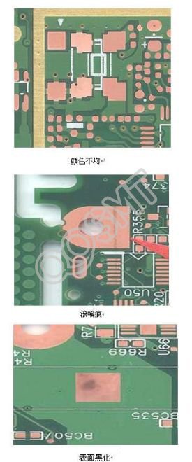
7) The most important thing to pay attention to when visually inspecting OSP (ENTEK) boards is the quality of the film, such as surface blackening, roller marks, uneven film thickness, and whether the bottom copper is oxidized. As shown in the picture below, it is unacceptable.
2. Immersion Silver surface treatment plate
1) There is no half-plug hole Via design. If you find a half-plug hole, please send an engineering confirmation inquiry.
2) Add Teardrop to the interface between PAD and lines.
3) Silver thickness: 5~16 µ”.
4) Thickness measurement position: PAD Size 40~80 mil.
5) Rework conditions: At most once, and the thickness of the silver after rework shall not exceed 5 ~ 16µ” and be recorded on the PCB for tracking.
6) Solder mask exposure conditions (UV bump after thermal cure under the solder mask) need to be matched with solder mask ink and suggestions according to the raw material supply recommendations; because the solder mask layer will be caused by its coverage in SMIA (Solder Mask Interface Area) The problem of liquid medicine residue. Therefore, special attention must be paid to the quality of the solder mask covering the surface.
7) Vision Inspection Points: A visual inspection station will be added after the chemical silver process is completed, and the mandatory inspection items with a magnifying glass of more than 10 times are: the surface color of the chemical silver, whether it is discolored or oxidized.
8) BGA area: Whether the interface between the BGA PAD and the circuit is intact, whether it is thinned or broken.
9) SMIA area: Whether the interface between PAD and the thinnest line is complete, whether it is thinned or broken. The above is the inspection of the first and last pieces of each batch, and is included in the independent inspection items.
3. Lead-free tin spray surface treatment board (LF HASL)
1) The thickness of spray tin is 100~1000 μ”.
2) It must be cleaned with IPA before shipment. The IPA concentration is 25% +/-5%.
3) Ion contamination test: <4μg.
4) Number of reworks: at most once, and recorded on the PCB for easy tracking.