• HOME

  • Products

  • Support

  • Blog

  • About Us

  • Contact Us

  • SMT Feeder

  • SMT Nozzle

  • Pick And Place Machine

  • SMT Machine Part

  • Stencil Printer & Inspection Machine

  • Reflow Oven & Wave Solder

  • SMT Peripheral Equipment

  • SMT Consumables

  • YAMAHA Tape Feeder

  • JUKI Tape Feeder

  • Samsung Tape Feeder

  • FUJI Tape Feeder

  • Panasonic Tape Feeder

  • Siemens Tape Feeder

  • SMT Label Feeder

  • SMT Stick Feeder

  • SMT Feeder Parts

  • SMT Feeder Cart

  • YAMAHA Nozzle

  • JUKI Nozzle

  • Samsung Nozzle

  • FUJI Nozzle

  • Panasonic Nozzle

  • ASM/Siemens Nozzle

  • Yamaha Pick And Place Machine

  • JUKI Pick And Place Machine

  • Samsung Pick And Place Machine

  • FUJI Pick And Place Machine

  • Panasonic Pick And Place Machine

  • ASM/Siemens Pick And Place Machine

  • Samsung Mounter Part

  • JUKI Mounter Part

  • Yamaha Mounter Part

  • Fuji Mounter Part

  • Panasonic Mounter Part

  • ASM/Siemens Mounter Part

  • Printer Part

  • Reflow Oven Part

  • Wave Soldering Part

  • Binding/Die Bonding Machine Part

  • GKG Automatic Stencil Printer

  • DESEN Automatic Stencil printer

  • DEK Automatic Stencil Printer

  • Semi Automatic Stencil Printer

  • SAKI AOI Inspection Machine

  • SinicTek SPI Inspection Machine

  • TRI SPI Inspection Machine

  • TRI AOI Inspection Machine

  • Heller Reflow Oven

  • Ersa Reflow Oven

  • Ersa Wave Solder Machine

  • ETC Reflow Oven

  • TAMURA Reflow Oven

  • Vitronics Soltec Reflow Oven

  • BTU Reflow Oven

  • Thermal Profiler

  • Small Equipment

  • IC Tray

  • Loader and Unloader Machine

  • Conveyor Machine

  • Traffic Controllers

  • Buffers

  • Cleaning Machine

  • Feeder Calibration Instrument

  • Splicing Tools

  • ESD Products

  • Splicing Tape

  • ASM Spare Parts

  • PCB Thimble

  • Printing Scraper

  • After Sales

  • Download

  • FAQ

  • News & Events

  • Video Library

  • Technical Articles

Toggle navigation

PCBPCBA BGA common design problem case description

Jan 24, 2024
In daily work, we often encounter the problem of poor BGA welding due to improper PCB design. Therefore, today I will make a summary of several common types of design problems. I hope everyone can provide valuable opinions!


There are mainly the following phenomena:


1. The vias at the bottom of the BGA are not processed.


There are via holes in the BGA pad, and the solder balls are lost with the solder during the welding process; the solder mask process is not implemented in PCB production, resulting in the loss of solder and solder balls through the via holes adjacent to the pads, resulting in missing solder balls, as shown in the figure below .


2. The BGA solder mask is poorly designed.


Placing via holes on the PCB pad will cause solder loss; in high-density assembly, micro-hole, blind hole or plug hole processes must be adopted to avoid solder loss; as shown in the figure below, wave soldering is used, and there are via holes at the bottom of the BGA. After wave soldering, the solder on the via holes affects the reliability of BGA soldering, causing defects such as short circuits in components.


3. BGA pad design.


The lead-out line of the BGA pad should not exceed 50% of the diameter of the pad, and the lead-out line of the power pad should not be less than 0.1mm before it can be thickened. In order to prevent the pad from deforming, the solder mask opening should not be larger than 0.05mm, as shown in the figure below.


4. The pad size is not standardized, too large or too small, as shown in the figure below.


5. BGA pads are of different sizes, and the solder joints are irregular circles of different sizes, as shown in the figure below.


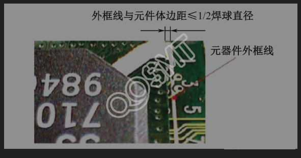
6. The distance between the BGA frame line and the edge of the component body is too small.


All parts of the component should be within the range of the marking line, and the distance between the frame line and the edge of the component package should be greater than 1/2 of the soldering end size of the component, as shown in the figure below.

Request for quotation and Quotes Average quote returned in under 1 work day.
Invoice and Packing Slip Average invoice and packing slip returned in under 1 work day.
Shipment Spare Parts delivered on average 3-7 work days after receipt of payment. (Via DHL, UPS, FedEx, and TNT)
Desktop Website